- 您現(xiàn)在的位置:買賣IC網(wǎng) > PDF目錄25635 > MQ80C32E-36SC (TEMIC SEMICONDUCTORS) 8-BIT, 36 MHz, MICROCONTROLLER, CQFP44 PDF資料下載
參數(shù)資料
| 型號: | MQ80C32E-36SC |
| 廠商: | TEMIC SEMICONDUCTORS |
| 元件分類: | 微控制器/微處理器 |
| 英文描述: | 8-BIT, 36 MHz, MICROCONTROLLER, CQFP44 |
| 文件頁數(shù): | 65/198頁 |
| 文件大小: | 4822K |
| 代理商: | MQ80C32E-36SC |
第1頁第2頁第3頁第4頁第5頁第6頁第7頁第8頁第9頁第10頁第11頁第12頁第13頁第14頁第15頁第16頁第17頁第18頁第19頁第20頁第21頁第22頁第23頁第24頁第25頁第26頁第27頁第28頁第29頁第30頁第31頁第32頁第33頁第34頁第35頁第36頁第37頁第38頁第39頁第40頁第41頁第42頁第43頁第44頁第45頁第46頁第47頁第48頁第49頁第50頁第51頁第52頁第53頁第54頁第55頁第56頁第57頁第58頁第59頁第60頁第61頁第62頁第63頁第64頁當(dāng)前第65頁第66頁第67頁第68頁第69頁第70頁第71頁第72頁第73頁第74頁第75頁第76頁第77頁第78頁第79頁第80頁第81頁第82頁第83頁第84頁第85頁第86頁第87頁第88頁第89頁第90頁第91頁第92頁第93頁第94頁第95頁第96頁第97頁第98頁第99頁第100頁第101頁第102頁第103頁第104頁第105頁第106頁第107頁第108頁第109頁第110頁第111頁第112頁第113頁第114頁第115頁第116頁第117頁第118頁第119頁第120頁第121頁第122頁第123頁第124頁第125頁第126頁第127頁第128頁第129頁第130頁第131頁第132頁第133頁第134頁第135頁第136頁第137頁第138頁第139頁第140頁第141頁第142頁第143頁第144頁第145頁第146頁第147頁第148頁第149頁第150頁第151頁第152頁第153頁第154頁第155頁第156頁第157頁第158頁第159頁第160頁第161頁第162頁第163頁第164頁第165頁第166頁第167頁第168頁第169頁第170頁第171頁第172頁第173頁第174頁第175頁第176頁第177頁第178頁第179頁第180頁第181頁第182頁第183頁第184頁第185頁第186頁第187頁第188頁第189頁第190頁第191頁第192頁第193頁第194頁第195頁第196頁第197頁第198頁
157
8111C–MCU Wireless–09/09
AT86RF231
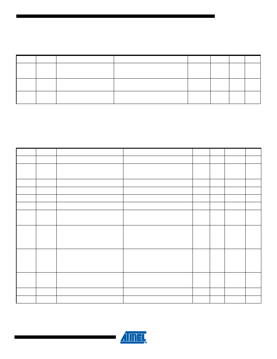
12.3
Digital Pin Characteristics
.Test Conditions: T
OP = 25°C (unless otherwise stated)
Note:
1. The capacitive load should not be larger than 50 pF for all I/Os when using the default driver strength settings, refer to Sec-
tion 1.3.1 “Driver Strength Settings” on page 7. Generally, large load capacitances increase the overall current consumption.
12.4
Digital Interface Timing Characteristics
Test Conditions: T
OP = 25°C, VDD = 3.0V, CL = 50 pF (unless otherwise stated).
Table 12-3.
Digital Pin Characteristics
No.
Symbol
Parameter
Condition
Min.
Typ.
Max
Units
12.3.1
V
IH
High level input voltage(1)
V
DD - 0.4
V
12.3.2
VIL
Low level input voltage(1)
0.4
V
12.3.3
V
OH
High level output voltage(1)
For all output driver strengths defined
in TRX_CTRL_0
V
DD - 0.4
V
12.3.4
VOL
Low level output voltage(1)
For all output driver strengths defined
in TRX_CTRL_0
0.4
V
Table 12-4.
Digital Interface Timing Characteristics
No.
Symbol
Parameter
Condition
Min.
Typ.
Max
Units
12.4.1
f
sync
SCLK frequency
synchronous operation
8
MHz
12.4.2
fasync
SCLK frequency
asynchronous operation
7.5
MHz
12.4.3
t1
/SEL low to MISO active
180
ns
12.4.4
t
2
SCLK to MISO out
data hold time
10
ns
12.4.5
t3
MOSI setup time
10
ns
12.4.6
t
4
MOSI hold time
10
ns
12.4.7
t
5
LSB last byte to MSB next byte
250(2)
ns
12.4.8
t6
/SEL high to MISO tri state
10
ns
12.4.9
t
7
SLP_TR pulse width
TX start trigger
62.5
Note(1)
ns
12.4.10
t
8
SPI idle time
(SEL rising to falling edge)
SPI read/write, standard SRAM
and Frame Buffer access modes,
Idle time between consecutive SPI
accesses
250
ns
12.4.11
t
8
SPI idle time
(SEL rising to falling edge)
SPI Fast SRAM read/write access
mode, refer to Section 11.1.5,
Idle time between consecutive SPI
accesses
500
ns
12.4.12
t9
Last SCLK to /SEL high
250
ns
12.4.13
t
10
Reset pulse width
10 clock cycles at 16 MHz
625
ns
12.4.14
t11
SPI access latency after reset
10 clock cycles at 16 MHz
625
ns
12.4.15
t12
AES core cycle time
24
s
相關(guān)PDF資料 |
PDF描述 |
|---|---|
| MR80C52XXX-20:R | 8-BIT, MROM, 20 MHz, MICROCONTROLLER, CQCC44 |
| MQ80C32E-30/883 | 8-BIT, 30 MHz, MICROCONTROLLER, CQFP44 |
| MR80C52CXXX-16/883R | 8-BIT, MROM, 16 MHz, MICROCONTROLLER, CQCC44 |
| MR80C52TXXX-16SB | 8-BIT, MROM, 16 MHz, MICROCONTROLLER, CQCC44 |
| MD83C154TXXX-L16P883D | 8-BIT, MROM, 16 MHz, MICROCONTROLLER, CDIP40 |
相關(guān)代理商/技術(shù)參數(shù) |
參數(shù)描述 |
|---|---|
| MQ82370-20 | 制造商:Rochester Electronics LLC 功能描述:- Bulk |
| MQ8238020 | 制造商:Intel 功能描述:CONTROLLER: OTHER |
| MQ82380-20 | 制造商:Rochester Electronics LLC 功能描述:- Bulk |
| MQ82380-20/R | 制造商:Rochester Electronics LLC 功能描述: |
| MQ82592 | 制造商:Rochester Electronics LLC 功能描述:- Bulk |
發(fā)布緊急采購,3分鐘左右您將得到回復(fù)。