- 您現(xiàn)在的位置:買賣IC網(wǎng) > PDF目錄371047 > MC68HC08AS32AFU (MOTOROLA INC) Microcontrollers PDF資料下載
參數(shù)資料
| 型號(hào): | MC68HC08AS32AFU |
| 廠商: | MOTOROLA INC |
| 元件分類: | 微控制器/微處理器 |
| 英文描述: | Microcontrollers |
| 中文描述: | 8-BIT, MROM, 8.4 MHz, MICROCONTROLLER, PQFP64 |
| 封裝: | QFP-64 |
| 文件頁數(shù): | 165/296頁 |
| 文件大?。?/td> | 2291K |
| 代理商: | MC68HC08AS32AFU |
第1頁第2頁第3頁第4頁第5頁第6頁第7頁第8頁第9頁第10頁第11頁第12頁第13頁第14頁第15頁第16頁第17頁第18頁第19頁第20頁第21頁第22頁第23頁第24頁第25頁第26頁第27頁第28頁第29頁第30頁第31頁第32頁第33頁第34頁第35頁第36頁第37頁第38頁第39頁第40頁第41頁第42頁第43頁第44頁第45頁第46頁第47頁第48頁第49頁第50頁第51頁第52頁第53頁第54頁第55頁第56頁第57頁第58頁第59頁第60頁第61頁第62頁第63頁第64頁第65頁第66頁第67頁第68頁第69頁第70頁第71頁第72頁第73頁第74頁第75頁第76頁第77頁第78頁第79頁第80頁第81頁第82頁第83頁第84頁第85頁第86頁第87頁第88頁第89頁第90頁第91頁第92頁第93頁第94頁第95頁第96頁第97頁第98頁第99頁第100頁第101頁第102頁第103頁第104頁第105頁第106頁第107頁第108頁第109頁第110頁第111頁第112頁第113頁第114頁第115頁第116頁第117頁第118頁第119頁第120頁第121頁第122頁第123頁第124頁第125頁第126頁第127頁第128頁第129頁第130頁第131頁第132頁第133頁第134頁第135頁第136頁第137頁第138頁第139頁第140頁第141頁第142頁第143頁第144頁第145頁第146頁第147頁第148頁第149頁第150頁第151頁第152頁第153頁第154頁第155頁第156頁第157頁第158頁第159頁第160頁第161頁第162頁第163頁第164頁當(dāng)前第165頁第166頁第167頁第168頁第169頁第170頁第171頁第172頁第173頁第174頁第175頁第176頁第177頁第178頁第179頁第180頁第181頁第182頁第183頁第184頁第185頁第186頁第187頁第188頁第189頁第190頁第191頁第192頁第193頁第194頁第195頁第196頁第197頁第198頁第199頁第200頁第201頁第202頁第203頁第204頁第205頁第206頁第207頁第208頁第209頁第210頁第211頁第212頁第213頁第214頁第215頁第216頁第217頁第218頁第219頁第220頁第221頁第222頁第223頁第224頁第225頁第226頁第227頁第228頁第229頁第230頁第231頁第232頁第233頁第234頁第235頁第236頁第237頁第238頁第239頁第240頁第241頁第242頁第243頁第244頁第245頁第246頁第247頁第248頁第249頁第250頁第251頁第252頁第253頁第254頁第255頁第256頁第257頁第258頁第259頁第260頁第261頁第262頁第263頁第264頁第265頁第266頁第267頁第268頁第269頁第270頁第271頁第272頁第273頁第274頁第275頁第276頁第277頁第278頁第279頁第280頁第281頁第282頁第283頁第284頁第285頁第286頁第287頁第288頁第289頁第290頁第291頁第292頁第293頁第294頁第295頁第296頁
Input/Output (I/O) Ports
Port E
MC68HC08AS32A — Rev. 1
Data Sheet
MOTOROLA
Input/Output (I/O) Ports
165
12.6 Port E
Port E is an 8-bit special-function port that shares two of its pins with the timer
interface module (TIM), two of its pins with the serial communications interface
module (SCI), and four of its pins with the serial peripheral interface module (SPI).
12.6.1 Port E Data Register
The port E data register contains a data latch for each of the eight port E pins.
PTE[7:0] — Port E Data Bits
PTE[7:0] are read/write, software programmable bits. Data direction of each
port E pin is under the control of the corresponding bit in data direction
register E.
SPSCK — SPI Serial Clock Bit
The PTE7/SPSCK
pin is the serial clock input of an SPI slave module and serial
clock output of an SPI master module. When the SPE bit is clear, the
PTE7/SPSCK pin is available for general-purpose I/O.
MOSI — Master Out/Slave In Bit
The PTE6/MOSI pin is the master out/slave in terminal of the SPI module. When
the SPE bit is clear, the PTE6/MOSI pin is available for general-purpose I/O.
(See
15.13.1 SPI Control Register
.)
MISO — Master In/Slave Out Bit
The PTE5/MISO pin is the master in/slave out terminal of the SPI module. When
the SPI enable bit, SPE, is clear, the SPI module is disabled, and the
PTE5/MISO pin is available for general-purpose I/O. (See
15.13.1 SPI Control
Register
.)
SS — Slave Select Bit
The PTE4/SS pin is the slave select input of the SPI module. When the SPE bit
is clear or when the SPI master bit, SPMSTR, is set and MODFEN bit is low, the
PTE4/SS pin is available for general-purpose I/O. (See
15.12.4 SS (Slave
Select)
.) When the SPI is enabled as a slave, the DDRE4 bit in data direction
register E (DDRE) has no effect on the PTE4/SS pin.
NOTE:
Data direction register E (DDRE) does not affect the data direction of port E pins
that are being used by the SPI module. However, the DDRE bits always determine
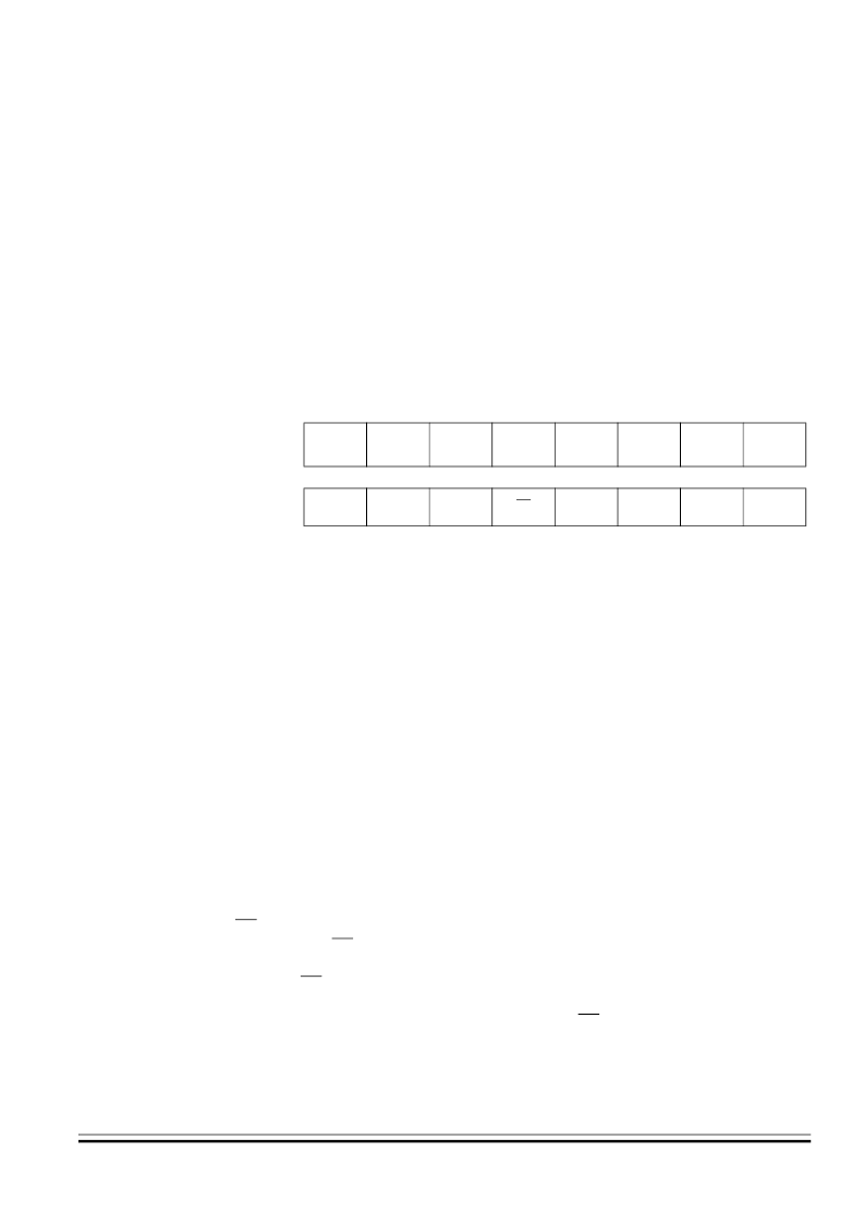
Address:
$0008
Bit 7
6
5
4
3
2
1
Bit 0
Read:
PTE7
PTE6
PTE5
PTE4
PTE3
PTE2
PTE1
PTE0
Write:
Reset:
Alternate
Function:
SPSCK
MOSI
MISO
SS
TCH1
TCH0
RxD
TxD
Figure 12-14. Port E Data Register (PTE)
F
Freescale Semiconductor, Inc.
For More Information On This Product,
Go to: www.freescale.com
n
.
相關(guān)PDF資料 |
PDF描述 |
|---|---|
| MC68HC08AS32AVFU | Microcontrollers |
| MC68HC08AS32CAFN | Microcontrollers |
| MC68HC08AS32VAFN | Microcontrollers |
| MC68HC08AS32A | Microcontrollers |
| MC68HC08AS32ACFU | Microcontrollers |
相關(guān)代理商/技術(shù)參數(shù) |
參數(shù)描述 |
|---|---|
| MC68HC08AZ0 | 制造商:MOTOROLA 制造商全稱:Motorola, Inc 功能描述:Advance Information |
| MC68HC08AZ0CFU | 制造商:MOTOROLA 制造商全稱:Motorola, Inc 功能描述:Advance Information |
| MC68HC08AZ16 | 制造商:MOTOROLA 制造商全稱:Motorola, Inc 功能描述:HCMOS Microcontroller Unit |
| MC68HC08AZ24 | 制造商:MOTOROLA 制造商全稱:Motorola, Inc 功能描述:HCMOS Microcontroller Unit |
| MC68HC08AZ32 | 制造商:FREESCALE 制造商全稱:Freescale Semiconductor, Inc 功能描述:Advance Information |
發(fā)布緊急采購,3分鐘左右您將得到回復(fù)。