- 您現(xiàn)在的位置:買賣IC網(wǎng) > PDF目錄98068 > S1C6S3L2D0A0100 4-BIT, MROM, 0.032768 MHz, MICROCONTROLLER, UUC79 PDF資料下載
參數(shù)資料
| 型號: | S1C6S3L2D0A0100 |
| 元件分類: | 微控制器/微處理器 |
| 英文描述: | 4-BIT, MROM, 0.032768 MHz, MICROCONTROLLER, UUC79 |
| 封裝: | DIE-79 |
| 文件頁數(shù): | 229/271頁 |
| 文件大小: | 1542K |
| 代理商: | S1C6S3L2D0A0100 |
第1頁第2頁第3頁第4頁第5頁第6頁第7頁第8頁第9頁第10頁第11頁第12頁第13頁第14頁第15頁第16頁第17頁第18頁第19頁第20頁第21頁第22頁第23頁第24頁第25頁第26頁第27頁第28頁第29頁第30頁第31頁第32頁第33頁第34頁第35頁第36頁第37頁第38頁第39頁第40頁第41頁第42頁第43頁第44頁第45頁第46頁第47頁第48頁第49頁第50頁第51頁第52頁第53頁第54頁第55頁第56頁第57頁第58頁第59頁第60頁第61頁第62頁第63頁第64頁第65頁第66頁第67頁第68頁第69頁第70頁第71頁第72頁第73頁第74頁第75頁第76頁第77頁第78頁第79頁第80頁第81頁第82頁第83頁第84頁第85頁第86頁第87頁第88頁第89頁第90頁第91頁第92頁第93頁第94頁第95頁第96頁第97頁第98頁第99頁第100頁第101頁第102頁第103頁第104頁第105頁第106頁第107頁第108頁第109頁第110頁第111頁第112頁第113頁第114頁第115頁第116頁第117頁第118頁第119頁第120頁第121頁第122頁第123頁第124頁第125頁第126頁第127頁第128頁第129頁第130頁第131頁第132頁第133頁第134頁第135頁第136頁第137頁第138頁第139頁第140頁第141頁第142頁第143頁第144頁第145頁第146頁第147頁第148頁第149頁第150頁第151頁第152頁第153頁第154頁第155頁第156頁第157頁第158頁第159頁第160頁第161頁第162頁第163頁第164頁第165頁第166頁第167頁第168頁第169頁第170頁第171頁第172頁第173頁第174頁第175頁第176頁第177頁第178頁第179頁第180頁第181頁第182頁第183頁第184頁第185頁第186頁第187頁第188頁第189頁第190頁第191頁第192頁第193頁第194頁第195頁第196頁第197頁第198頁第199頁第200頁第201頁第202頁第203頁第204頁第205頁第206頁第207頁第208頁第209頁第210頁第211頁第212頁第213頁第214頁第215頁第216頁第217頁第218頁第219頁第220頁第221頁第222頁第223頁第224頁第225頁第226頁第227頁第228頁當(dāng)前第229頁第230頁第231頁第232頁第233頁第234頁第235頁第236頁第237頁第238頁第239頁第240頁第241頁第242頁第243頁第244頁第245頁第246頁第247頁第248頁第249頁第250頁第251頁第252頁第253頁第254頁第255頁第256頁第257頁第258頁第259頁第260頁第261頁第262頁第263頁第264頁第265頁第266頁第267頁第268頁第269頁第270頁第271頁
I-46
EPSON
S1C6S3N2 TECHNICAL HARDWARE
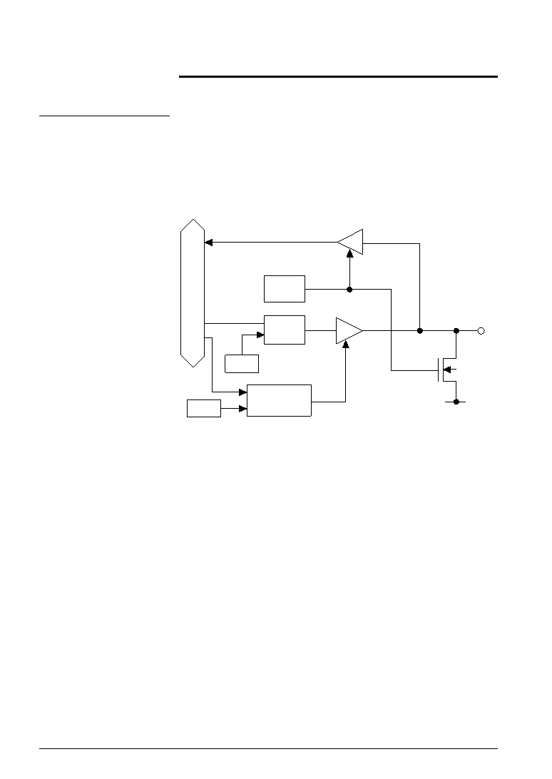
CHAPTER 4: PERIPHERAL CIRCUITS AND OPERATION (I/O Ports)
I/O Ports (P00–P03, P10–P13)
The S1C6S3N2 Series has general-purpose I/O ports (4 bits
x
2). Figure 4.6.1 shows the configuration of the I/O ports.
The four bits of each of the I/O ports P00–P03 and P10–P13
can be set to either input mode or output mode. Modes can
be set by writing data to the I/O control register.
4.6
Configuration of
I/O ports
Address
Register
Input
control
I/O control
register
Data
bus
Address
P
VSS
Fig. 4.6.1
Configuration of I/O ports
相關(guān)PDF資料 |
PDF描述 |
|---|---|
| S1C6S3L2F0A0100 | 4-BIT, MROM, 0.032768 MHz, MICROCONTROLLER, PQFP80 |
| S1C6S3N2F0A0100 | 4-BIT, MROM, 0.032768 MHz, MICROCONTROLLER, PQFP80 |
| S1C6S3N7F | 4-BIT, MROM, 0.08 MHz, MICROCONTROLLER, PQFP60 |
| S1C6S460D | 4-BIT, MROM, 2 MHz, MICROCONTROLLER, UUC124 |
| S1C88104P0A0100 | 8-BIT, MROM, 8.2 MHz, MICROCONTROLLER, PBGA240 |
相關(guān)代理商/技術(shù)參數(shù) |
參數(shù)描述 |
|---|---|
| S1C7309X | 制造商:SAMSUNG 制造商全稱:Samsung semiconductor 功能描述:B/W CCD PROCESSOR |
| S1C7309X01 | 制造商:SAMSUNG 制造商全稱:Samsung semiconductor 功能描述:B/W CCD PROCESSOR |
| S1C88349 | 制造商:EPSON 制造商全稱:EPSON 功能描述:8-bit Single Chip Microcomputer |
| S1C88649 | 制造商:EPSON 制造商全稱:EPSON 功能描述:8-bit Single Chip Microcomputer |
| S1C88650 | 制造商:EPSON 制造商全稱:EPSON 功能描述:8-bit Single Chip Microcomputer |
發(fā)布緊急采購,3分鐘左右您將得到回復(fù)。