- 您現(xiàn)在的位置:買賣IC網(wǎng) > PDF目錄383236 > L6374FP (意法半導(dǎo)體) INDUSTRIAL QUAD LINE DRIVER PDF資料下載
參數(shù)資料
| 型號(hào): | L6374FP |
| 廠商: | 意法半導(dǎo)體 |
| 英文描述: | INDUSTRIAL QUAD LINE DRIVER |
| 中文描述: | 工業(yè)四線路驅(qū)動(dòng)器 |
| 文件頁(yè)數(shù): | 12/13頁(yè) |
| 文件大?。?/td> | 179K |
| 代理商: | L6374FP |
第1頁(yè)第2頁(yè)第3頁(yè)第4頁(yè)第5頁(yè)第6頁(yè)第7頁(yè)第8頁(yè)第9頁(yè)第10頁(yè)第11頁(yè)當(dāng)前第12頁(yè)第13頁(yè)
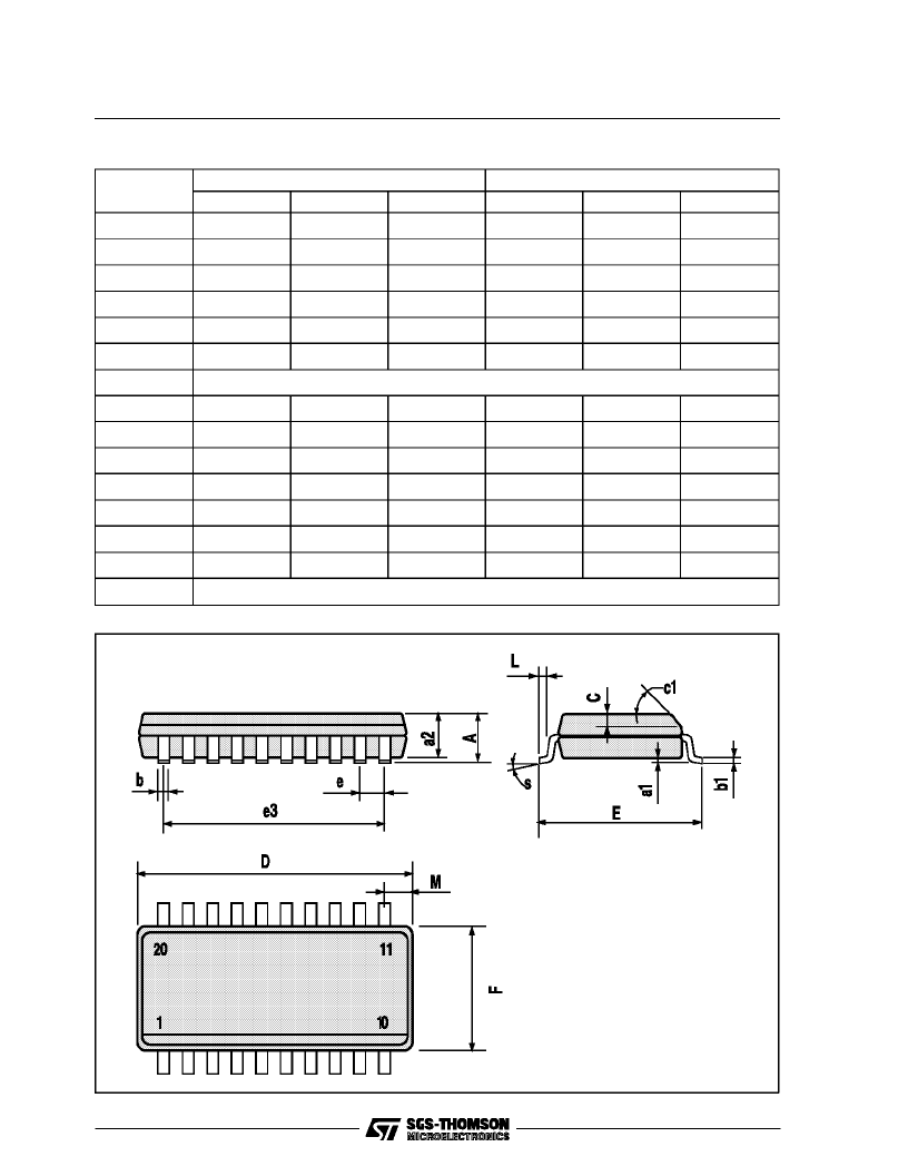
SO20PACKAGE MECHANICAL DATA
DIM.
mm
inch
MIN.
TYP.
MAX.
MIN.
TYP.
MAX.
A
2.65
0.104
a1
0.1
0.3
0.004
0.012
a2
2.45
0.096
b
0.35
0.49
0.014
0.019
b1
0.23
0.32
0.009
0.013
C
0.5
0.020
c1
45 (typ.)
D
12.6
13.0
0.496
0.512
E
10
10.65
0.394
0.419
e
1.27
0.050
e3
11.43
0.450
F
7.4
7.6
0.291
0.299
L
0.5
1.27
0.020
0.050
M
0.75
0.030
S
8 (max.)
L6374
12/13
相關(guān)PDF資料 |
PDF描述 |
|---|---|
| L6375 | 0.5A INDUSTRIAL INTELLIGENT POWER SWITCH |
| L6375D | 0.5A INDUSTRIAL INTELLIGENT POWER SWITCH |
| L6376 | 0.5A HIGH-SIDE DRIVER QUAD INTELLIGENT POWER SWITCH |
| L6376PD | 0.5A HIGH-SIDE DRIVER QUAD INTELLIGENT POWER SWITCH |
| L6377 | 0.5A High-Side Driver Intelligent Power Switch(0.5A高邊驅(qū)動(dòng)器智能功率開(kāi)關(guān)) |
相關(guān)代理商/技術(shù)參數(shù) |
參數(shù)描述 |
|---|---|
| L6374FP013TR | 功能描述:緩沖器和線路驅(qū)動(dòng)器 Industrial Quad Line RoHS:否 制造商:Micrel 輸入線路數(shù)量:1 輸出線路數(shù)量:2 極性:Non-Inverting 電源電壓-最大:+/- 5.5 V 電源電壓-最小:+/- 2.37 V 最大工作溫度:+ 85 C 安裝風(fēng)格:SMD/SMT 封裝 / 箱體:MSOP-8 封裝:Reel |
| L6374FPT | 制造商:STMICROELECTRONICS 制造商全稱:STMicroelectronics 功能描述:Industrial quad line driver |
| L6375 | 制造商:STMICROELECTRONICS 制造商全稱:STMicroelectronics 功能描述:0.5A INDUSTRIAL INTELLIGENT POWER SWITCH |
| L6375D | 功能描述:功率驅(qū)動(dòng)器IC 0.5A IND Intelligent Pwr Switch RoHS:否 制造商:Micrel 產(chǎn)品:MOSFET Gate Drivers 類型:Low Cost High or Low Side MOSFET Driver 上升時(shí)間: 下降時(shí)間: 電源電壓-最大:30 V 電源電壓-最小:2.75 V 電源電流: 最大功率耗散: 最大工作溫度:+ 85 C 安裝風(fēng)格:SMD/SMT 封裝 / 箱體:SOIC-8 封裝:Tube |
| L6375D013TR | 功能描述:功率驅(qū)動(dòng)器IC Step Down Controller RoHS:否 制造商:Micrel 產(chǎn)品:MOSFET Gate Drivers 類型:Low Cost High or Low Side MOSFET Driver 上升時(shí)間: 下降時(shí)間: 電源電壓-最大:30 V 電源電壓-最小:2.75 V 電源電流: 最大功率耗散: 最大工作溫度:+ 85 C 安裝風(fēng)格:SMD/SMT 封裝 / 箱體:SOIC-8 封裝:Tube |
發(fā)布緊急采購(gòu),3分鐘左右您將得到回復(fù)。