- 您現(xiàn)在的位置:買賣IC網(wǎng) > PDF目錄67763 > M37643M8-XXXHP 8-BIT, MROM, 12 MHz, MICROCONTROLLER, PQFP80 PDF資料下載
參數(shù)資料
| 型號: | M37643M8-XXXHP |
| 元件分類: | 微控制器/微處理器 |
| 英文描述: | 8-BIT, MROM, 12 MHz, MICROCONTROLLER, PQFP80 |
| 封裝: | 12 X 12 MM, 0.50 MM PITCH, PLASTIC, LQFP-80 |
| 文件頁數(shù): | 27/120頁 |
| 文件大?。?/td> | 1253K |
| 代理商: | M37643M8-XXXHP |
第1頁第2頁第3頁第4頁第5頁第6頁第7頁第8頁第9頁第10頁第11頁第12頁第13頁第14頁第15頁第16頁第17頁第18頁第19頁第20頁第21頁第22頁第23頁第24頁第25頁第26頁當(dāng)前第27頁第28頁第29頁第30頁第31頁第32頁第33頁第34頁第35頁第36頁第37頁第38頁第39頁第40頁第41頁第42頁第43頁第44頁第45頁第46頁第47頁第48頁第49頁第50頁第51頁第52頁第53頁第54頁第55頁第56頁第57頁第58頁第59頁第60頁第61頁第62頁第63頁第64頁第65頁第66頁第67頁第68頁第69頁第70頁第71頁第72頁第73頁第74頁第75頁第76頁第77頁第78頁第79頁第80頁第81頁第82頁第83頁第84頁第85頁第86頁第87頁第88頁第89頁第90頁第91頁第92頁第93頁第94頁第95頁第96頁第97頁第98頁第99頁第100頁第101頁第102頁第103頁第104頁第105頁第106頁第107頁第108頁第109頁第110頁第111頁第112頁第113頁第114頁第115頁第116頁第117頁第118頁第119頁第120頁
14
SINGLE-CHIP 8-BIT CMOS MICROCOMPUTER
MITSUBISHI MICROCOMPUTERS
7643 Group
PRELIMINAR
Y
Notice:
This
is not
a final
specification.
Some
parametric
limits
are
subject
to
change.
I/O PORTS
Direction Registers
The I/O ports P0–P8 have direction registers which determine the
input/output direction of each individual pin. Each bit in a direction
register corresponds to one pin, each pin can be set to be input port
or output port.
When “0” is written to the bit corresponding to a pin, that pin be-
comes an input pin. When “1” is written to that bit, that pin becomes
an output pin.
If data is read from a pin set to output, the value of the port output
latch is read, not the value of the pin itself. Pins set to input are float-
ing. If a pin set to input is written to, only the port output latch is
written to and the pin remains floating.
Slew Rate Control
By setting bits 0 to 5 of the port control register (address 001016) to
“1”, slew rate control is enabled. VIHL or CMOS level can be used as
a port P2 input level.
Pull-up Control
By setting the port P2 pull-up control register (address 001216), pull-
up of each pin of port P2 can be controlled with a program.
However, the contents of port P2 pull-up control register do not affect
ports programmed as the output ports but as the input ports.
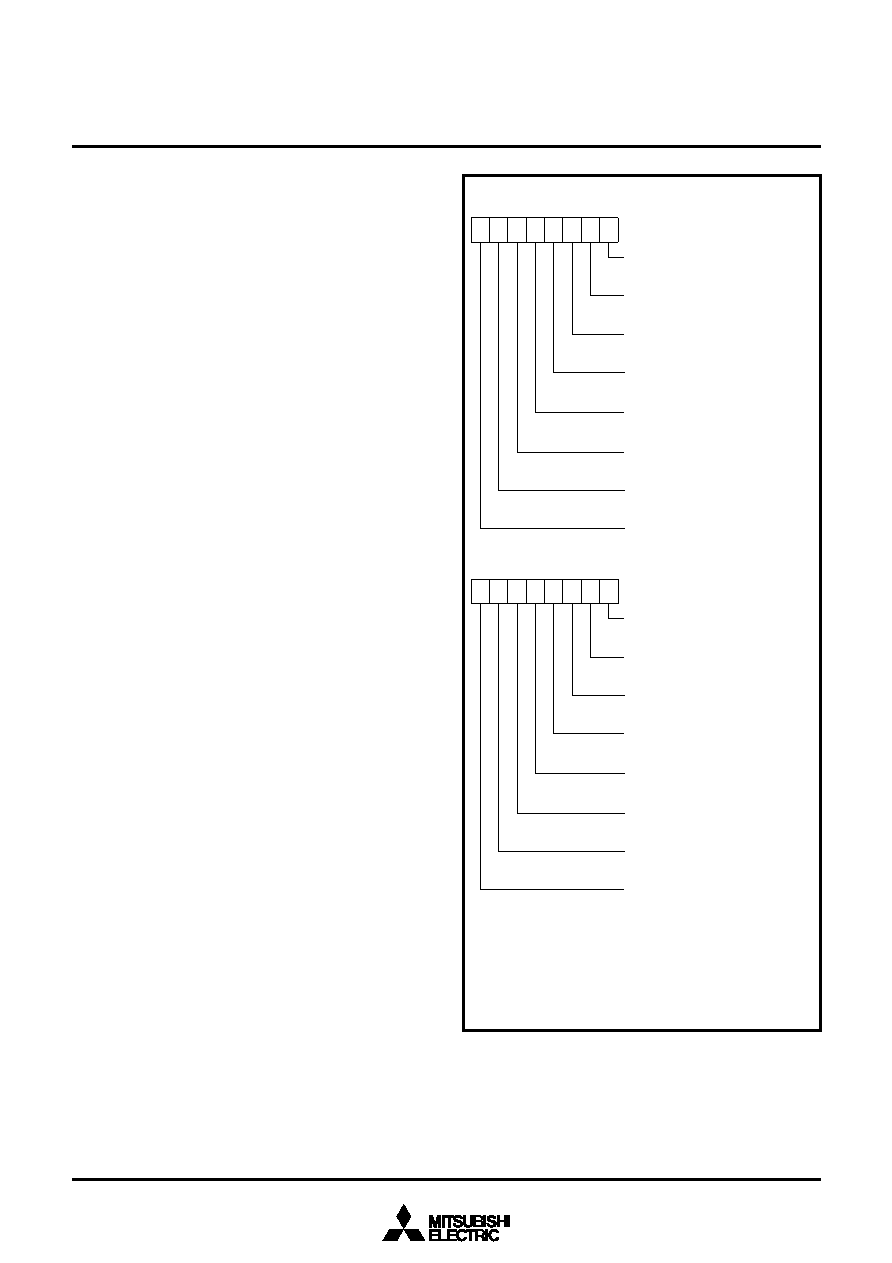
Fig. 11 Structure of port control and port P2 pull-up control
registers
Port control register (address 001016)
PTC
Port P0 to P3 slew rate control bit (Note 1)
0: Disabled
1: Enabled
Port P4 slew rate control bit (Note 1)
0: Disabled
1: Enabled
Port P5 slew rate control bit (Note 1)
0: Disabled
1: Enabled
Port P6 slew rate control bit (Note 1)
0: Disabled
1: Enabled
Port P7 slew rate control bit (Note 1)
0: Disabled
1: Enabled
Port P8 slew rate control bit (Note 1)
0: Disabled
1: Enabled
Port P2 input level select bit
0: Reduced VIHL level input (Note 2)
1: CMOS level input
Reserved bit (“0” at read/write)
Notes 1: The slew rate function can reduce di/dt by modifying an internal
buffer structure.
2: The characteristics of VIHL level is basically the same as that of
TTL level. But, its switching center point is a little higher than
TTL’s. Refer to section “Recommended operating conditions”.
b0
b7
Port P2 pull-up control register
(address 001216) PUP2
b0
b7
Port P20 pull-up control bit
0: Disabled
1: Enabled
Port P21 pull-up control bit
0: Disabled
1: Enabled
Port P22 pull-up control bit
0: Disabled
1: Enabled
Port P23 pull-up control bit
1: Enabled
Port P24 pull-up control bit
0: Disabled
1: Enabled
Port P25 pull-up control bit
0: Disabled
1: Enabled
Port P26 pull-up control bit
0: Disabled
1: Enabled
Port P27 pull-up control bit
0: Disabled
1: Enabled
0
相關(guān)PDF資料 |
PDF描述 |
|---|---|
| M37702S1LGP | 16-BIT, 8 MHz, MICROCONTROLLER, PQFP80 |
| M37702M2LXXXGP | 16-BIT, MROM, 8 MHz, MICROCONTROLLER, PQFP80 |
| M37702M2LXXXHP | 16-BIT, MROM, 8 MHz, MICROCONTROLLER, PQFP80 |
| M37703MDBSP | 16-BIT, MROM, 25 MHz, MICROCONTROLLER, PDIP64 |
| M37721S1BFP | 16-BIT, 25 MHz, MICROCONTROLLER, PQFP100 |
相關(guān)代理商/技術(shù)參數(shù) |
參數(shù)描述 |
|---|---|
| M3764A-12 | 制造商:OK International 功能描述: |
| M3765 | 制造商:未知廠家 制造商全稱:未知廠家 功能描述:HORN/SIREN WITH SOFT CHIRP 6 ALARM SOUNDS |
| M3766 | 制造商:未知廠家 制造商全稱:未知廠家 功能描述:HORN/SIREN WITH SOFT CHIRP 6 ALARM SOUNDS |
| M37702E2LGP | 制造商:Mitsubishi Electric 功能描述: |
| M37702E4BFS | 制造商:Renesas Electronics Corporation 功能描述:EPROM MCU/8BIT CMOS EMULATION CHIP - Bulk |
發(fā)布緊急采購,3分鐘左右您將得到回復(fù)。