- 您現(xiàn)在的位置:買賣IC網(wǎng) > PDF目錄361036 > LM98501CCVBH (NATIONAL SEMICONDUCTOR CORP) 10-Bit, 27 MSPS Camera Signal Processor PDF資料下載
參數(shù)資料
| 型號: | LM98501CCVBH |
| 廠商: | NATIONAL SEMICONDUCTOR CORP |
| 元件分類: | 消費家電 |
| 英文描述: | 10-Bit, 27 MSPS Camera Signal Processor |
| 中文描述: | SPECIALTY CONSUMER CIRCUIT, PQFP48 |
| 封裝: | LQFP-48 |
| 文件頁數(shù): | 6/24頁 |
| 文件大小: | 490K |
| 代理商: | LM98501CCVBH |
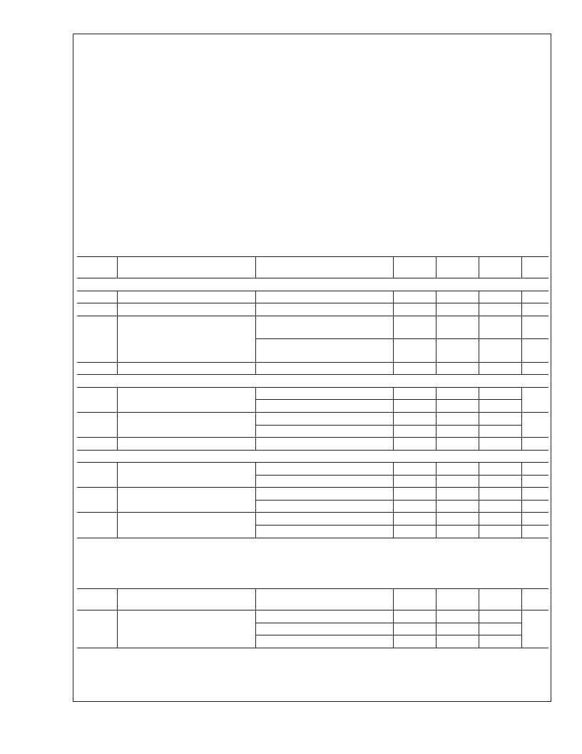
Absolute Maximum Ratings
(Notes 1, 2)
If Military/Aerospace specified devices are required,
please contact the National Semiconductor Sales Office/
Distributors for availability and specifications.
Any Positive Supply Voltage
Voltage on Any Input or Output Pin
Input Current at Any Pin (Note 3)
Package Input Current (Note 3)
Package Dissipation at T
A
= 25C
(Note 4)
ESD Susceptibility (Note 5)
Human Body Model
Machine Model
Soldering Temperature Infrared,
10 seconds (Note 6)
4.2V
0.3V to +4.2V
±
35 mA
±
50 mA
2000V
200V
260C
Storage Temperature
65C to +150C
Operating Ratings
(Notes 1, 2)
Operating Temperature Range
All Supply Voltages
V
IN
Voltage Range
V
REFT
Voltage Range
V
REFB
Voltage Range
V
REFP
Voltage Range
V
REFN
Voltage Range
All Digital Inputs Voltage Range
0C
≤
T
A
≤
+70C
+2.7V to +3.3V
0.0V to AV+
2.0V to 2.5V
0.4V to 0.9V
1.3V to 1.9V
1.3V to 1.9V
0.05V to +3.35V
DC and Logic Level Specifications
The following specifications apply for DV+ = AV+ = DV + I/O = +3.0V, C
= 10 pF, and f
CLK
= 27 MHz unless otherwise
noted.
Boldface limits apply for T
A
= T
MIN
to T
MAX
:
all other limits T
A
= 25C (Note 7).
Symbol
Parameter
Conditions
Min
(Note 9)
Typical
(Note 8)
Max
(Note 9)
Units
DIGITAL INPUT CHARACTERISTICS
V
IH
Logical “1” Input Voltage
V
IL
Logical “0” Input Voltage
I
IH
Logical “1” Input Current
2.0
V
V
1.0
V
IH
= DV+, Digital Inputs Except
Reset
V
IH
= DV+, Reset (internal
pull-down resistor)
V
IL
= DGND
100
nA
400
μA
I
IL
DIGITAL OUTPUT CHARACTERISTICS
V
OH
Logical “1” Output Voltage
Logical “0” Input Current
100
nA
DV+ = 3.3V, I
OUT
= 0.5 mA
DV+ = 2.7V, I
OUT
= 0.5 mA
DV+ = 3.3V, I
OUT
= 1.6 mA
DV+ = 2.7V, I
OUT
= 1.6 mA
2.5
2.3
V
V
OL
Logical “0” Output Voltage
0.4
0.4
V
I
OS
POWER SUPPLY CHARACTERISTICS
IA
Analog Supply Current
Output Short Circuit Current
30
mA
P
D
= LOW
P
D
= HIGH
P
D
= LOW
P
D
= HIGH
P
D
= LOW
P
D
= HIGH
56.8
3.1
6.5
0.1
2.3
0.1
mA
mA
mA
mA
mA
mA
5.0
ID
Digital Supply Current
1.0
ID I/O
Digital Output Driver Supply
Current
1.0
Power Dissipation Specifications
The following specifications apply for DV+ = AV+ = DV + I/O = +3.0V, C
= 10 pF, and f
CLK
= 27 MHz unless otherwise
noted.
Boldface limits apply for T
A
= T
MIN
to T
MAX
:
all other limits T
A
= 25C (Note 7).
Symbol
Parameter
Conditions
Min
(Note 9)
Typical
(Note 8)
150
195
240
Max
(Note 9)
Units
PWR
Average Power Dissipation
AV+ = DV+ = DV+ I/O = 2.7V
AV+ = DV+ = DV+ I/O = 3.0V
AV+ = DV+ = DV+ I/O = 3.3V
mW
L
www.national.com
6
相關(guān)PDF資料 |
PDF描述 |
|---|---|
| LM98501 | 10-Bit, 27 MSPS Camera Signal Processor |
| LMC555CBPEVAL | CMOS Timer |
| LMC555CN | CMOS Timer |
| LMC555 | CMOS Timer |
| LMC555CM | CMOS Timer |
相關(guān)代理商/技術(shù)參數(shù) |
參數(shù)描述 |
|---|---|
| LM98501VBH WAF | 制造商:Texas Instruments 功能描述: |
| LM98502A WAF | 制造商:Texas Instruments 功能描述: |
| LM98503 | 制造商:NSC 制造商全稱:National Semiconductor 功能描述:10-Bit, 18 MSPS Camera Signal Processor |
| LM98503CCVV | 制造商:NSC 制造商全稱:National Semiconductor 功能描述:10-Bit, 18 MSPS Camera Signal Processor |
| LM98510CCMT | 制造商:Rochester Electronics LLC 功能描述: 制造商:Texas Instruments 功能描述: |
發(fā)布緊急采購,3分鐘左右您將得到回復(fù)。