- 您現(xiàn)在的位置:買賣IC網 > PDF目錄361035 > LM9800CCV (NATIONAL SEMICONDUCTOR CORP) 8-Bit Greyscale/24-Bit Color Linear CCD Sensor Processor PDF資料下載
參數資料
| 型號: | LM9800CCV |
| 廠商: | NATIONAL SEMICONDUCTOR CORP |
| 元件分類: | 模擬信號調理 |
| 英文描述: | 8-Bit Greyscale/24-Bit Color Linear CCD Sensor Processor |
| 中文描述: | SPECIALTY ANALOG CIRCUIT, PQCC52 |
| 封裝: | PLASTIC, LCC-52 |
| 文件頁數: | 28/34頁 |
| 文件大?。?/td> | 619K |
| 代理商: | LM9800CCV |
第1頁第2頁第3頁第4頁第5頁第6頁第7頁第8頁第9頁第10頁第11頁第12頁第13頁第14頁第15頁第16頁第17頁第18頁第19頁第20頁第21頁第22頁第23頁第24頁第25頁第26頁第27頁當前第28頁第29頁第30頁第31頁第32頁第33頁第34頁
Applications Information
(Continued)
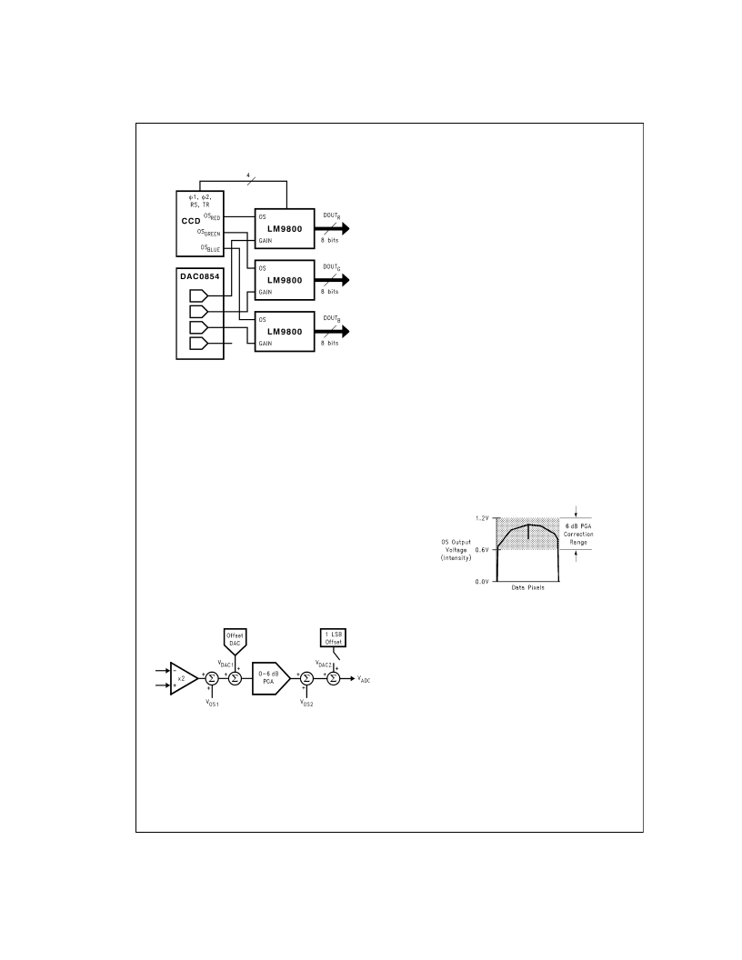
5.3 Parallel Output CCD, Three LM9800s
Figure 36 uses three LM9800s to achieve a 7.5Mpixel/sec
(2.5M RGB pixels/sec) pixel rate. The three LM9800s are
synchronized by applying the same MCLK and SYNC sig-
nals to all three devices. One LM9800 provides the clock sig-
nals required for the CCD. Since the coefficient data for all
three LM9800s will be latched simultaneously on the rising
edge of CCLK, the correction coefficient bus should either be
at least 21 bits wide (7 correction coefficient bits by 3
LM9800s) or run at a 7.5MHz rate and latched into a buffer
between the correction coefficient databus and each
LM9800. Similarly, the output data for all three LM9800s will
be available simultaneously at the 3 output databusses.
6.0 CALIBRATION
To calibrate a LM9800-based system, follow these steps:
6.1 Offset Calibration
This procedure corrects for offsets generated inside the
LM9800. Because the LM9800 uses CDS to eliminate the
pixel-to-pixel offset errors of the CCD, very good results can
be obtained even if this procedure is not implemented. In this
case the Offset DAC and Offset Add bit are simply set to 0.
To use the Offset DAC and Offset Add bit for offset correc-
tion, the offset errors must first be determined. This is done
be measuring the voltage at the PGA output, using the ADC.
If this voltage is known with a PGA gain of x1 (0 dB) and x2
(6 dB), then the offset errors (V
and V
OS2
) can be deter-
mined from the following two equations:
V
ADC1
=
1(V
OS1
+ V
DAC1
) + V
OS2
+ V
DAC2
(PGA gain = x1)
V
ADC2
=
2(V
OS1
+ V
DAC1
) + V
OS2
+ V
DAC2
(PGA gain = x2)
Solving for V
OS1
and V
OS2
:
V
OS1
= (V
ADC2
–V
ADC1
)–V
DAC1
V
OS2
= (2V
ADC1
–V
ADC2
)–V
DAC2
These equations were used to produce this procedure for
cancelling the LM9800’s offset errors:
1.
Turn off the VGA.
2.
Set the Offset DAC to +7 LSB. (This is done to ensure
the total offset is positive and therefore measurable by
the ADC.)
3.
Set the Offset Add bit to 0.
4.
Set the PGA Gain to x1 (PGA code = 0).
5.
Digitize a black line.
6.
Calculate the average (in ADC LSBs) of all the valid pix-
els in the black line and store that number as “B1”
(equivalent to V
ADC1
).
7.
Set the PGA Gain to x2 (PGA code = 127).
8.
Digitize a black line.
9.
Calculate the average (in ADC LSBs) of all the valid pix-
els in the black line and store that number as “B2”
(equivalent to V
ADC2
).
10. Program the Offset DAC using the formula:
Offset DAC code = 7+B1–B2.
11. If 2B1
>
B2, then set the OffsetAdd bit to 0. If 2B1
<
B2,
set the Offset Add bit to 1.
6.2 Coarse Gain Calibration
The LM9800’s PGA corrects for up to 6 dB of varIation in the
CCD output signal’s white level intensity. That 6 dB range
has to be centered inside the 6 dB window of correction.
With the VGA off and the PGA set to a gain of 0 dB, the
LM9800 expects the maximum CCD white level output to be
below 1.2V (V
) corresponding to strong pixels, and the
minimum white level output voltage to be above 0.6V (V
IN
/2), corresponding to weaker CCD pixels or pixels further
from the light source. If the variation for a white input is inside
this range, as shown in Figure 38 the PGA can correct for it
and linearize it.
If the maximum white level voltage (the voltage from the
strongest pixels) is greater than 1.2V (Figure 39) the
LM9800 will be unable to linearize the CCD’s output.
DS012498-43
FIGURE 36. Parallel Output CCD, Three LM9800s
DS012498-54
FIGURE 37. Offset Calibration
DS012498-44
FIGURE 38. CCD Input Signal In Range
www.national.com
28
相關PDF資料 |
PDF描述 |
|---|---|
| LM9811CCVF | 10-Bit Greyscale/30-Bit Color Linear CCD Sensor Processor |
| LM9811 | 10-Bit Greyscale/30-Bit Color Linear CCD Sensor Processor |
| LM9811CCV | 10-Bit Greyscale/30-Bit Color Linear CCD Sensor Processor |
| LM9831CCVJD | LM9831 42-Bit Color, 1200dpi USB Image Scanner |
| LM9831 | LM9831 42-Bit Color, 1200dpi USB Image Scanner |
相關代理商/技術參數 |
參數描述 |
|---|---|
| LM9800CCVF | 制造商:未知廠家 制造商全稱:未知廠家 功能描述:Special Function Video Processor |
| LM9801 | 制造商:NSC 制造商全稱:National Semiconductor 功能描述:Greyscale/24-Bit Color Linear CCD Sensor Processor |
| LM9801CCV | 制造商:NSC 制造商全稱:National Semiconductor 功能描述:Greyscale/24-Bit Color Linear CCD Sensor Processor |
| LM9801CCVF | 制造商:NSC 制造商全稱:National Semiconductor 功能描述:Greyscale/24-Bit Color Linear CCD Sensor Processor |
| LM980-SC3 | 功能描述:基本/快動開關 Foot Switch RoHS:否 制造商:Omron Electronics 觸點形式:SPDT 執(zhí)行器:Lever 電流額定值:5 A 電壓額定值 AC:250 V 電壓額定值 DC:30 V 功率額定值: 工作力:120 g IP 等級:IP 67 NEMA 額定值: 端接類型:Wire 安裝:Panel |
發(fā)布緊急采購,3分鐘左右您將得到回復。