- 您現(xiàn)在的位置:買賣IC網(wǎng) > PDF目錄358809 > LM12434CIWM (NATIONAL SEMICONDUCTOR CORP) Sign Data Acquisition System with Serial I/O and Self-Calibration PDF資料下載
參數(shù)資料
| 型號: | LM12434CIWM |
| 廠商: | NATIONAL SEMICONDUCTOR CORP |
| 元件分類: | 模擬信號調(diào)理 |
| 英文描述: | Sign Data Acquisition System with Serial I/O and Self-Calibration |
| 中文描述: | SPECIALTY ANALOG CIRCUIT, PDSO28 |
| 封裝: | SOP-28 |
| 文件頁數(shù): | 42/80頁 |
| 文件大小: | 1561K |
| 代理商: | LM12434CIWM |
第1頁第2頁第3頁第4頁第5頁第6頁第7頁第8頁第9頁第10頁第11頁第12頁第13頁第14頁第15頁第16頁第17頁第18頁第19頁第20頁第21頁第22頁第23頁第24頁第25頁第26頁第27頁第28頁第29頁第30頁第31頁第32頁第33頁第34頁第35頁第36頁第37頁第38頁第39頁第40頁第41頁當(dāng)前第42頁第43頁第44頁第45頁第46頁第47頁第48頁第49頁第50頁第51頁第52頁第53頁第54頁第55頁第56頁第57頁第58頁第59頁第60頁第61頁第62頁第63頁第64頁第65頁第66頁第67頁第68頁第69頁第70頁第71頁第72頁第73頁第74頁第75頁第76頁第77頁第78頁第79頁第80頁
7.0 Digital Interface
(Continued)
In both cases the data transfer is insensitive to idle state of
the SCLK. SCLK can stay at either logic level high or low
when not clocking (see Figure 11)
Data transfer in this mode is basically byte-oriented. This is
compatible with the serial interface of the target microcon-
trolIers and microprocessors. As mentioned, the LM12434
and LM12
à
L
ó
438 have three different communication cy-
cles: write cycle, read cycle and burst read cycle. At the
start of each data transfer cycle, ‘‘command byte’’ is written
to the serial DAS, followed by write or read data. The com-
mand byte informs the LM12434 and LM12
à
L
ó
438 about
the communication cycle. The command byte carries the
following information:
D what type of data transfer (communication cycle) is start-
ed
D which device register to be accessed
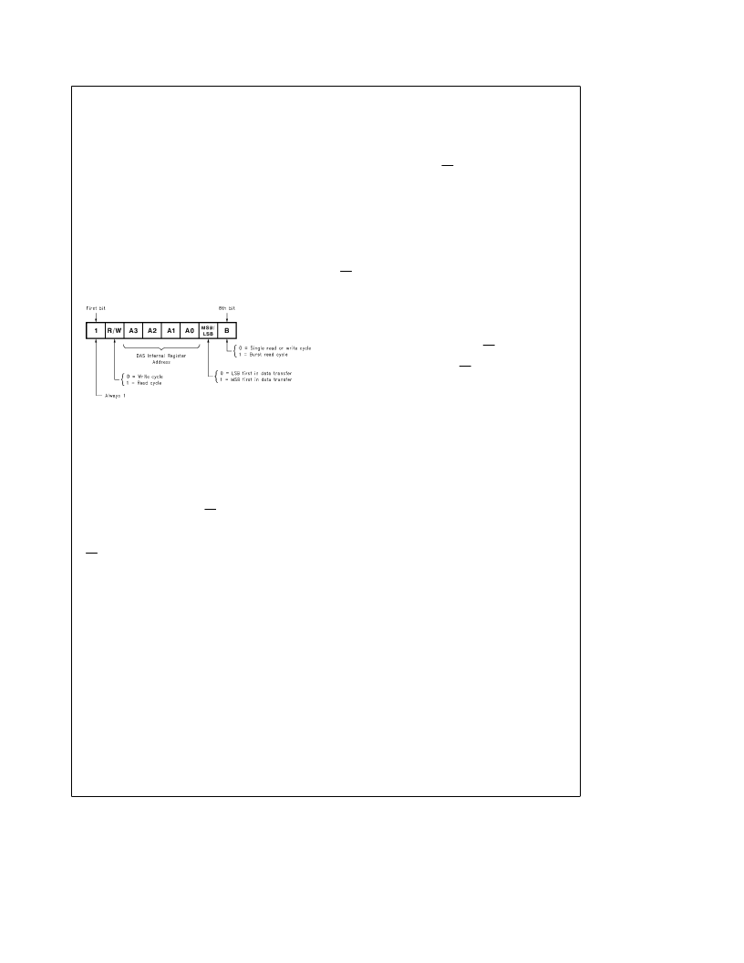
The command byte has the following format:
TL/H/11879–52
Note that the first bit may be either the MSB or the LSB of
the byte depending on the processor type, but it must be the
first bit transmitted to the LM12434 and LM12
à
L
ó
438.
Figure 11 shows the timing diagrams for different communi-
cation cycles. Figures 11a, b, c, d show write cycles for
various combinations of R/F pin logic level and SCLK idle
state. Figures 11e, f, g, h show read cycles for similar sets
of conditions. Figure 11i shows a burst read cycle for the
case of R/F
e
0 and low SCLK idle state. Note that these
timing diagrams depict general relationships between the
SCLK edges, the data bits and CS. These diagrams are not
meant to show guaranteed timing. (See specification tables
for parametric switching characteristics.)
Write cycle:
A write cycle begins with the falling edge of
CS. Then a command byte is written to the DAS on the DI
line synchronized by SCLK. The command byte has the
R/W and B bits equal to zero. Following the command byte,
16 bits of data (2 bytes) is shifted in on the same DI line.
This data is written to the register addressed in the com-
mand byte (A3, A2, A1, A0). The data is interpreted as MSB
or LSB first based on the logic level of the 7th bit (MSB/
LSB) in the command byte. There is no activity on the DO
line during write cycles and the DAS leaves the DO line in
the high impedance state. CS will go high after the transfer
of the last bit, thus completing the write cycle.
Read cycle:
A read cycle starts the same way as a write
cycle, except that the command byte’s R/W bits equal to
one. Following the command byte, the DAS outputs the
data on the DO line synchronized with the microcontroller’s
SCLK. The data is read from the register addressed in the
command byte. Data is shifted out MSB or LSB first, de-
pending on the logic level of the MSB/LSB bit. The logic
state of the Dl line is ‘‘don’t care’’ after the command byte.
CS will go high after the transfer of the last data bit, then
completing the read cycle.
Burst read cycle:
A burst read cycle starts the same way
as a single read cycle, but the B bit in the command byte is
set to one, indicating a burst read cycle. Following the com-
mand byte the data is output on the DO line as long as the
DAS receives SCLK from the system. To tell the DAS when
a burst read cycle is completed pull CS high after the 8th
and before the 15th SCLK cycle during the last data byte
transfer (seeFigure 11i ). After CS high is detected and the
last data bit is transferred, the DAS is ready for a new com-
munication cycle to begin.
The timing diagrams in Figure 11 show the transfer of data
in packets of 8 bits (bytes). This represents the way the
serial ports of most microcontrollers and microprocessors
produce serial clock and data. The DAS does not require a
gap between the first and second byte of the data; 16 con-
tinuous clock cycles will transfer the data word. However,
there should be a gap equal to 3 CLK (the DAS main clock
input, not the SCLK) cycles between the end of the com-
mand byte and the start of the data during a read cycle. This
is not a concern in most systems for two reasons. First, the
processor generally has some inherent gap between byte
transfers. Second, the SCLK frequency is usually signifi-
cantly slower than the CLK frequency. For example, a
68HC11 processor with an 8 MHz crystal generates a maxi-
mum SCLK frequency of 1 MHz. If the DAS is running with a
6 MHz CLK, there are 6 cycles of CLK within each cycle of
SCLK and the requirement is satisfied even if SCLK oper-
ates continuously during and after the command byte.
42
相關(guān)PDF資料 |
PDF描述 |
|---|---|
| LM12454 | General Purpose Controller Z84C15 |
| LM12454 | 12-Bit Sign Data Acquisition System with Self-Calibration |
| LM12454CIV | 12-Bit Sign Data Acquisition System with Self-Calibration |
| LM124AFK | CAP .0039UF 50V PPS FILM 1206 2% |
| LM324PT | OP-AMP|QUAD|BIPOLAR|TSSOP|14PIN|PLASTIC |
相關(guān)代理商/技術(shù)參數(shù) |
參數(shù)描述 |
|---|---|
| LM12438CIV | 制造商:NSC 制造商全稱:National Semiconductor 功能描述:Sign Data Acquisition System with Serial I/O and Self-Calibration |
| LM12438CIWM | 制造商:NSC 制造商全稱:National Semiconductor 功能描述:Sign Data Acquisition System with Serial I/O and Self-Calibration |
| LM12454 | 制造商:未知廠家 制造商全稱:未知廠家 功能描述:General Purpose Controller Z84C15 |
| LM12454_06 | 制造商:NSC 制造商全稱:National Semiconductor 功能描述:12-Bit + Sign Data Acquisition System with Self-Calibration |
| LM12454A WAF | 制造商:Texas Instruments 功能描述: |
發(fā)布緊急采購,3分鐘左右您將得到回復(fù)。