- 您現(xiàn)在的位置:買(mǎi)賣(mài)IC網(wǎng) > PDF目錄377639 > LFX1200B-03F900I (LATTICE SEMICONDUCTOR CORP) The ispXPGA architecture PDF資料下載
參數(shù)資料
| 型號(hào): | LFX1200B-03F900I |
| 廠商: | LATTICE SEMICONDUCTOR CORP |
| 元件分類(lèi): | FPGA |
| 英文描述: | The ispXPGA architecture |
| 中文描述: | FPGA, 3844 CLBS, 1250000 GATES, PBGA900 |
| 封裝: | FPBGA-900 |
| 文件頁(yè)數(shù): | 6/89頁(yè) |
| 文件大小: | 941K |
| 代理商: | LFX1200B-03F900I |
第1頁(yè)第2頁(yè)第3頁(yè)第4頁(yè)第5頁(yè)當(dāng)前第6頁(yè)第7頁(yè)第8頁(yè)第9頁(yè)第10頁(yè)第11頁(yè)第12頁(yè)第13頁(yè)第14頁(yè)第15頁(yè)第16頁(yè)第17頁(yè)第18頁(yè)第19頁(yè)第20頁(yè)第21頁(yè)第22頁(yè)第23頁(yè)第24頁(yè)第25頁(yè)第26頁(yè)第27頁(yè)第28頁(yè)第29頁(yè)第30頁(yè)第31頁(yè)第32頁(yè)第33頁(yè)第34頁(yè)第35頁(yè)第36頁(yè)第37頁(yè)第38頁(yè)第39頁(yè)第40頁(yè)第41頁(yè)第42頁(yè)第43頁(yè)第44頁(yè)第45頁(yè)第46頁(yè)第47頁(yè)第48頁(yè)第49頁(yè)第50頁(yè)第51頁(yè)第52頁(yè)第53頁(yè)第54頁(yè)第55頁(yè)第56頁(yè)第57頁(yè)第58頁(yè)第59頁(yè)第60頁(yè)第61頁(yè)第62頁(yè)第63頁(yè)第64頁(yè)第65頁(yè)第66頁(yè)第67頁(yè)第68頁(yè)第69頁(yè)第70頁(yè)第71頁(yè)第72頁(yè)第73頁(yè)第74頁(yè)第75頁(yè)第76頁(yè)第77頁(yè)第78頁(yè)第79頁(yè)第80頁(yè)第81頁(yè)第82頁(yè)第83頁(yè)第84頁(yè)第85頁(yè)第86頁(yè)第87頁(yè)第88頁(yè)第89頁(yè)
Lattice Semiconductor
ispXPGA Family Data Sheet
6
Con
fi
gurable Logic Element
The CLE is made up of a four-input Look-up Table (LUT-4), a Carry Chain Generator (CCG), and a two-input AND
gate. The LUT-4 creates various combinatorial and memory elements, the CCG creates a single one-bit full adder,
and the two-input AND gate can expand the CCG to incorporate Booth Multiplier capability by feeding the output of
the AND gate to one of the inputs of the CCG.
Of the
fi
ve inputs that feed each CLE, two are dedicated inputs into each LUT-4 and the remaining three take on
varying functionality. The third and fourth inputs can be used as either inputs to the LUT-4 or as a Feed-Thru to the
CSE via the WLG. The
fi
fth input can be a data port when the LUT is con
fi
gured as Distributed Memory, a select
line for multiplexer operation, or a Feed-Thru directly to the CSE via the WLG (Figure 2).
Look-Up Table – Combinatorial Mode
In combinatorial mode, the LUT-4 can implement any logic function up to four inputs. By using the carry chain and
the WLG, each LUT-4 can be combined to form the enhanced functions listed in Table 3.
Look-Up Table – Distributed Memory Mode
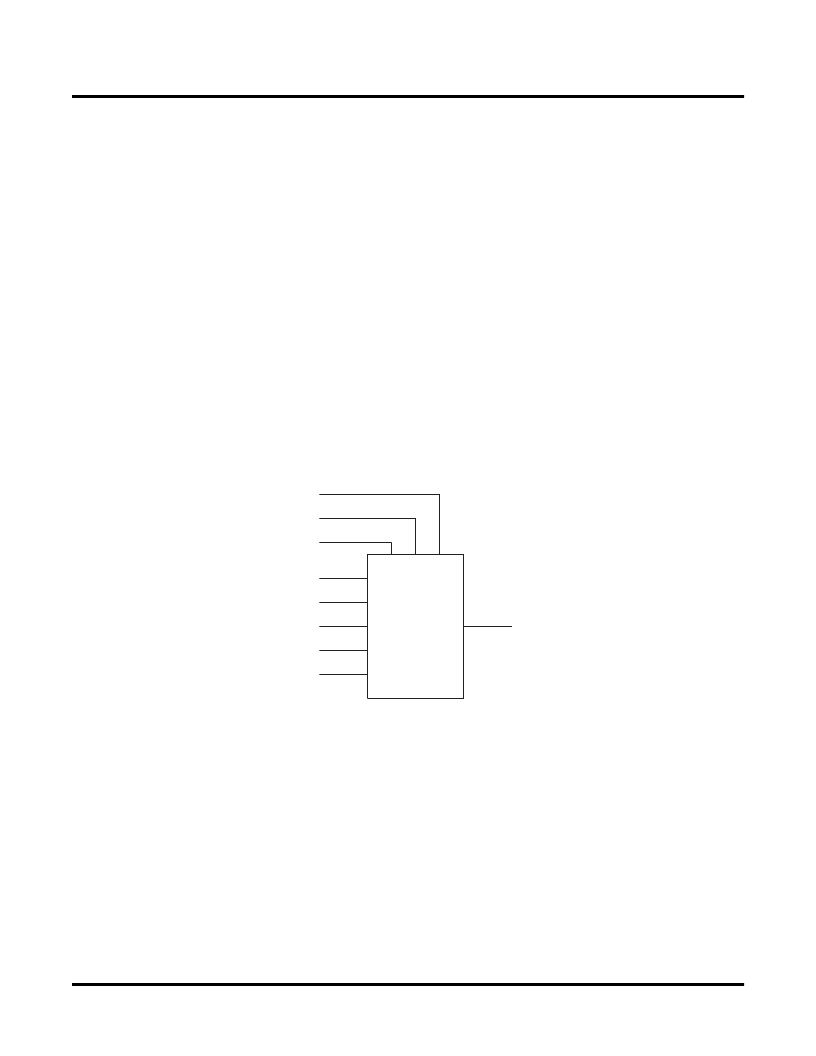
In the distributed memory mode, the LUT functions as a memory element. The inputs to the LUT function as
Address and Data. Each PFU is capable of implementing up to 64 SRAM bits. Both single and double port RAM
can be performed in the PFU (Table 3). Furthermore, the distributed memory can be con
fi
gured as either synchro-
nous or asynchronous memory. Figure 3 illustrates the LUT while in distributed memory mode. When using any
LUT in the PFU in memory mode, the Set/Reset signal will be used for Write Enable (WE(SR)) and the CLK0 signal
will be used as the clock for synchronous read and write.
Figure 3. LUT in Distributed Memory Mode
Look-Up Table – Shift Register Mode
In the shift register mode, the LUT functions as a 1-bit to 8-bit shift register. This means that each PFU can imple-
ment up to four 8-bit shift registers or any cascaded combination. Figure 4 illustrates the LUT when con
fi
gured in
shift register mode.
LUT-4
ADDR[0] (IN0)
PFUCLK0
ADDR[1] (IN1)
ADDR[2] (IN2)
ADDR[3] (IN3)
CEB0
WE (SR)
DOUT (4A)
DIN (SEL)
相關(guān)PDF資料 |
PDF描述 |
|---|---|
| LFX1200B-04F900C | The ispXPGA architecture |
| LFX1200C-4F900C | The ispXPGA architecture |
| LFX125B-4F900C | The ispXPGA architecture |
| LFX200B-4F900C | The ispXPGA architecture |
| LFX500B-4F900C | The ispXPGA architecture |
相關(guān)代理商/技術(shù)參數(shù) |
參數(shù)描述 |
|---|---|
| LFX1200B-03FE680C | 功能描述:FPGA - 現(xiàn)場(chǎng)可編程門(mén)陣列 15376 LUT-4 496 I/O RoHS:否 制造商:Altera Corporation 系列:Cyclone V E 柵極數(shù)量: 邏輯塊數(shù)量:943 內(nèi)嵌式塊RAM - EBR:1956 kbit 輸入/輸出端數(shù)量:128 最大工作頻率:800 MHz 工作電源電壓:1.1 V 最大工作溫度:+ 70 C 安裝風(fēng)格:SMD/SMT 封裝 / 箱體:FBGA-256 |
| LFX1200B-03FEN680C | 功能描述:FPGA - 現(xiàn)場(chǎng)可編程門(mén)陣列 1.25M Gt ispJTAG 2. 5/3.3V -3 Spd RoHS:否 制造商:Altera Corporation 系列:Cyclone V E 柵極數(shù)量: 邏輯塊數(shù)量:943 內(nèi)嵌式塊RAM - EBR:1956 kbit 輸入/輸出端數(shù)量:128 最大工作頻率:800 MHz 工作電源電壓:1.1 V 最大工作溫度:+ 70 C 安裝風(fēng)格:SMD/SMT 封裝 / 箱體:FBGA-256 |
| LFX1200B-03FEN680C2 | 功能描述:FPGA - 現(xiàn)場(chǎng)可編程門(mén)陣列 15376 LUT-4 496 I/O RoHS:否 制造商:Altera Corporation 系列:Cyclone V E 柵極數(shù)量: 邏輯塊數(shù)量:943 內(nèi)嵌式塊RAM - EBR:1956 kbit 輸入/輸出端數(shù)量:128 最大工作頻率:800 MHz 工作電源電壓:1.1 V 最大工作溫度:+ 70 C 安裝風(fēng)格:SMD/SMT 封裝 / 箱體:FBGA-256 |
| LFX1200B-04F900C | 功能描述:FPGA - 現(xiàn)場(chǎng)可編程門(mén)陣列 15376 LUT-4 496 I/O RoHS:否 制造商:Altera Corporation 系列:Cyclone V E 柵極數(shù)量: 邏輯塊數(shù)量:943 內(nèi)嵌式塊RAM - EBR:1956 kbit 輸入/輸出端數(shù)量:128 最大工作頻率:800 MHz 工作電源電壓:1.1 V 最大工作溫度:+ 70 C 安裝風(fēng)格:SMD/SMT 封裝 / 箱體:FBGA-256 |
| LFX1200B-04FE680C | 功能描述:FPGA - 現(xiàn)場(chǎng)可編程門(mén)陣列 15376 LUT-4 496 I/O RoHS:否 制造商:Altera Corporation 系列:Cyclone V E 柵極數(shù)量: 邏輯塊數(shù)量:943 內(nèi)嵌式塊RAM - EBR:1956 kbit 輸入/輸出端數(shù)量:128 最大工作頻率:800 MHz 工作電源電壓:1.1 V 最大工作溫度:+ 70 C 安裝風(fēng)格:SMD/SMT 封裝 / 箱體:FBGA-256 |
發(fā)布緊急采購(gòu),3分鐘左右您將得到回復(fù)。