- 您現(xiàn)在的位置:買賣IC網(wǎng) > PDF目錄67755 > LC5511D POWER FACTOR CONTROLLER, 18 kHz SWITCHING FREQ-MAX, DIP7 PDF資料下載
參數(shù)資料
| 型號(hào): | LC5511D |
| 元件分類: | 穩(wěn)壓器 |
| 英文描述: | POWER FACTOR CONTROLLER, 18 kHz SWITCHING FREQ-MAX, DIP7 |
| 封裝: | DIP-8/7 |
| 文件頁(yè)數(shù): | 16/40頁(yè) |
| 文件大小: | 888K |
| 代理商: | LC5511D |
第1頁(yè)第2頁(yè)第3頁(yè)第4頁(yè)第5頁(yè)第6頁(yè)第7頁(yè)第8頁(yè)第9頁(yè)第10頁(yè)第11頁(yè)第12頁(yè)第13頁(yè)第14頁(yè)第15頁(yè)當(dāng)前第16頁(yè)第17頁(yè)第18頁(yè)第19頁(yè)第20頁(yè)第21頁(yè)第22頁(yè)第23頁(yè)第24頁(yè)第25頁(yè)第26頁(yè)第27頁(yè)第28頁(yè)第29頁(yè)第30頁(yè)第31頁(yè)第32頁(yè)第33頁(yè)第34頁(yè)第35頁(yè)第36頁(yè)第37頁(yè)第38頁(yè)第39頁(yè)第40頁(yè)
23
Allegro MicroSystems, Inc.
115 Northeast Cutoff
Worcester, Massachusetts 01615-0036 U.S.A.
1.508.853.5000; www.allegromicro.com
28106.02
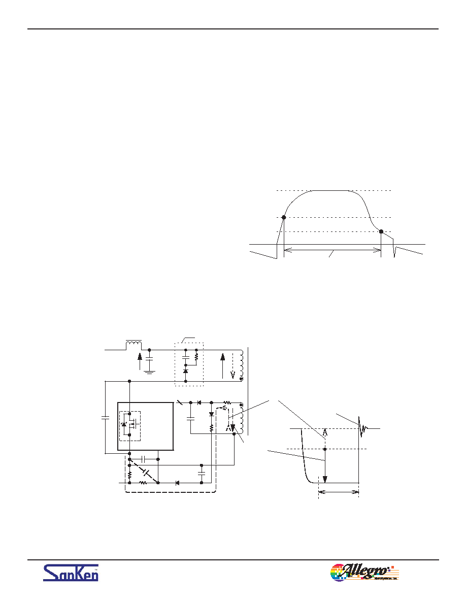
and provides positive voltage, the quasi-resonant signal, to the
OCP pin. After the power MOSFET turns off, the quasi-resonant
signal immediately goes up and it exceeds the Quasi-Resonant
Operation Threshold Voltage-1, VBD(TH1) = 0.24 V. After this
occurs, the power MOSFET remains off until the quasi-resonant
signal comes down enough to cross the Quasi-Resonant Opera-
tion Threshold Voltage-2, VBD(TH2) = 0.17 V. Then the power
MOSFET again turns on. In addition, at that point, VBD(TH1)
becomes effective again and it prevents malfunction of the quasi-
resonant operation from noise interference.
During that period, C7 must cause a delay time, tONDLY, such
that the power MOSFET turns on at the bottom point of VDS ; so
select an appropriate C7 value. R3 is recommended to be between
100 and 330 Ω, and C5 to be between 100 and 470 pF.
R4 must set the range for the quasi-resonant signal: greater than
or equal to VBD(TH1) under input and output conditions where VCC
becomes lowest, but less than the OCP Pin Overvoltage Protec-
tion (OVP) Threshold Voltage, VOCP(OVP) = 2.6 V, under condi-
tions where VCC becomes highest. Figure 30 shows the valid
period of the quasi-resonant signal. For initiating quasi-resonant
operation, the quasi-resonant signal pulse width between the
two points VBD(TH1) and VBD(TH2) , tQR, must be equal to its valid
period of 1.2 μs or more. This period must be ensured, while
at the same time the OCP pin peak voltage, VOCPPK , is recom-
mended to be between 1.5 and 2.0 V. Both conditions should be
satisfied throughout the power supply input and output ranges,
over variations in R3 and R4 actual component values.
Figure 29. OCP pin peripheral circuit and auxiliary winding voltage
Valid period tQR ≥1.2 μs
S/GND
VOCPPK,1.5 to 2.0 V recommended
VBD(TH1)= 0.24 V
VBD(TH2)= 0.17 V
Figure 30. Valid period of the quasi-resonant signal
8(1)
3(5)
1(2)
Auxiliary Winding Voltage
S/GND
D/ST
P
D
T
Forward Voltage
Flyback Voltage
EIN
Ef
Clamping Snubber
C2
EIN
L2
D5
R4
R3
VQR
C7
C3
C4
ROCP
D6
D7
C5
LC55xxD
(LC55xxF)
Erev1
Efw1
0 V
tON
R1
OCP
相關(guān)PDF資料 |
PDF描述 |
|---|---|
| LC5521D | 2.5 A POWER FACTOR CONTROLLER, 18 kHz SWITCHING FREQ-MAX, DIP7 |
| LC72137 | PLL FREQUENCY SYNTHESIZER, 40 MHz, PDIP22 |
| LC72137M | PLL FREQUENCY SYNTHESIZER, 40 MHz, PDSO20 |
| LC72137 | PLL FREQUENCY SYNTHESIZER, 40 MHz, PDIP22 |
| LC72137M | PLL FREQUENCY SYNTHESIZER, 40 MHz, PDSO20 |
相關(guān)代理商/技術(shù)參數(shù) |
參數(shù)描述 |
|---|---|
| LC5512B-10F256C | 功能描述:CPLD - 復(fù)雜可編程邏輯器件 PROGRAM EXPANDED LOG RoHS:否 制造商:Lattice 系列: 存儲(chǔ)類型:EEPROM 大電池?cái)?shù)量:128 最大工作頻率:333 MHz 延遲時(shí)間:2.7 ns 可編程輸入/輸出端數(shù)量:64 工作電源電壓:3.3 V 最大工作溫度:+ 90 C 最小工作溫度:0 C 封裝 / 箱體:TQFP-100 |
| LC5512B-10F256I | 功能描述:CPLD - 復(fù)雜可編程邏輯器件 PROGRAM EXPANDED LOG RoHS:否 制造商:Lattice 系列: 存儲(chǔ)類型:EEPROM 大電池?cái)?shù)量:128 最大工作頻率:333 MHz 延遲時(shí)間:2.7 ns 可編程輸入/輸出端數(shù)量:64 工作電源電壓:3.3 V 最大工作溫度:+ 90 C 最小工作溫度:0 C 封裝 / 箱體:TQFP-100 |
| LC5512B-10F484C | 功能描述:CPLD - 復(fù)雜可編程邏輯器件 Use ispMACH 4000B RoHS:否 制造商:Lattice 系列: 存儲(chǔ)類型:EEPROM 大電池?cái)?shù)量:128 最大工作頻率:333 MHz 延遲時(shí)間:2.7 ns 可編程輸入/輸出端數(shù)量:64 工作電源電壓:3.3 V 最大工作溫度:+ 90 C 最小工作溫度:0 C 封裝 / 箱體:TQFP-100 |
| LC5512B-10F484I | 功能描述:CPLD - 復(fù)雜可編程邏輯器件 Use ispMACH 4000B RoHS:否 制造商:Lattice 系列: 存儲(chǔ)類型:EEPROM 大電池?cái)?shù)量:128 最大工作頻率:333 MHz 延遲時(shí)間:2.7 ns 可編程輸入/輸出端數(shù)量:64 工作電源電壓:3.3 V 最大工作溫度:+ 90 C 最小工作溫度:0 C 封裝 / 箱體:TQFP-100 |
| LC5512B-10Q208C | 功能描述:CPLD - 復(fù)雜可編程邏輯器件 Use ispMACH 4000B RoHS:否 制造商:Lattice 系列: 存儲(chǔ)類型:EEPROM 大電池?cái)?shù)量:128 最大工作頻率:333 MHz 延遲時(shí)間:2.7 ns 可編程輸入/輸出端數(shù)量:64 工作電源電壓:3.3 V 最大工作溫度:+ 90 C 最小工作溫度:0 C 封裝 / 箱體:TQFP-100 |
發(fā)布緊急采購(gòu),3分鐘左右您將得到回復(fù)。