- 您現(xiàn)在的位置:買(mǎi)賣(mài)IC網(wǎng) > PDF目錄383238 > L6732 (意法半導(dǎo)體) Adjustable step-down controller with synchronous rectification PDF資料下載
參數(shù)資料
| 型號(hào): | L6732 |
| 廠商: | 意法半導(dǎo)體 |
| 英文描述: | Adjustable step-down controller with synchronous rectification |
| 中文描述: | 可調(diào)式降壓同步整流控制器 |
| 文件頁(yè)數(shù): | 16/33頁(yè) |
| 文件大?。?/td> | 735K |
| 代理商: | L6732 |
第1頁(yè)第2頁(yè)第3頁(yè)第4頁(yè)第5頁(yè)第6頁(yè)第7頁(yè)第8頁(yè)第9頁(yè)第10頁(yè)第11頁(yè)第12頁(yè)第13頁(yè)第14頁(yè)第15頁(yè)當(dāng)前第16頁(yè)第17頁(yè)第18頁(yè)第19頁(yè)第20頁(yè)第21頁(yè)第22頁(yè)第23頁(yè)第24頁(yè)第25頁(yè)第26頁(yè)第27頁(yè)第28頁(yè)第29頁(yè)第30頁(yè)第31頁(yè)第32頁(yè)第33頁(yè)
Device description
L6732
16/33
5.7
Driver section
The high-side and low-side drivers allow using different types of power MOSFETs (also multiple
MOSFETs to reduce the R
DSON
), maintaining fast switching transitions. The low-side driver is
supplied by V
CCDR
while the high-side driver is supplied by the BOOT pin. A predictive dead
time control avoids MOSFETs cross-conduction maintaining very short dead time duration in
the range of 20ns. The control monitors the phase node in order to sense the low-side body
diode recirculation. If the phase node voltage is less than a certain threshold (-350mV typ.)
during the dead time, it will be reduced in the next PWM cycle. The predictive dead time control
doesn't work when the high-side body diode is conducting because the phase node doesn't go
negative. This situation happens when the converter is sinking current for example and, in this
case, an adaptive dead time control operates.
5.8
Monitoring and protections
The output voltage is monitored by means of pin FB. If it is not within ±10% (typ.) of the
programmed value, the Power-Good (PGOOD) output is forced low.
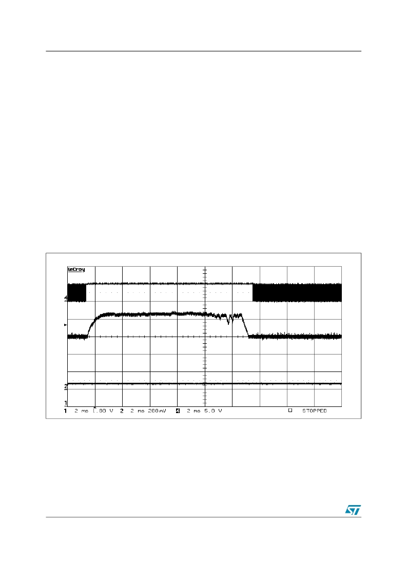
The device provides over-voltage-protection: when the voltage sensed on FB pin reaches a
value 20% (typ.) greater than the reference, the low-side driver is turned on as long as the over
voltage is detected (see
Figure 10.
).
It must be taken into account that there is an electrical network between the output terminal and
the FB pin and therefore the voltage at the pin is not a perfect replica of the output voltage.
However due to the fact that the converter can sink current, in the most of cases the low-side
will turn-on before the output voltage exceeds the over-voltage threshold, because the error
amplifier will throw off balance in advance. Even if the device doesn't report an over-voltage, the
behavior is the same, because the low-side is turned-on immediately. The following figure
shows the device behavior during an over-voltage event. The output voltage rises with a slope
of 100mV/μs, emulating in this way the breaking of the high-side MOSFET as an over-voltage
cause.
Figure 10. OVP
LGate
FB
相關(guān)PDF資料 |
PDF描述 |
|---|---|
| L6732TR | Adjustable step-down controller with synchronous rectification |
| L6902D013TR | RADIATION HARDENED HIGH EFFICIENCY, 5 AMP SWITCHING REGULATORS |
| L6902D | RADIATION HARDENED HIGH EFFICIENCY, 5 AMP SWITCHING REGULATORS |
| L6910 | ADJUSTABLE STEP DOWN CONTROLLER WITH SYNCHRONOUS RECTIFICATION |
| L6910A | ADJUSTABLE STEP DOWN CONTROLLER WITH SYNCHRONOUS RECTIFICATION |
相關(guān)代理商/技術(shù)參數(shù) |
參數(shù)描述 |
|---|---|
| L6732_08 | 制造商:STMICROELECTRONICS 制造商全稱:STMicroelectronics 功能描述:Adjustable step-down controller with synchronous rectification |
| L6732_0906 | 制造商:STMICROELECTRONICS 制造商全稱:STMicroelectronics 功能描述:Adjustable step-down controller with synchronous rectification |
| L6732C | 功能描述:DC/DC 開(kāi)關(guān)控制器 Adjustable Step Down Controller RoHS:否 制造商:Texas Instruments 輸入電壓:6 V to 100 V 開(kāi)關(guān)頻率: 輸出電壓:1.215 V to 80 V 輸出電流:3.5 A 輸出端數(shù)量:1 最大工作溫度:+ 125 C 安裝風(fēng)格: 封裝 / 箱體:CPAK |
| L6732CTR | 功能描述:開(kāi)關(guān)變換器、穩(wěn)壓器與控制器 Step-Dwn Controller RoHS:否 制造商:Texas Instruments 輸出電壓:1.2 V to 10 V 輸出電流:300 mA 輸出功率: 輸入電壓:3 V to 17 V 開(kāi)關(guān)頻率:1 MHz 工作溫度范圍: 安裝風(fēng)格:SMD/SMT 封裝 / 箱體:WSON-8 封裝:Reel |
| L6732TR | 功能描述:DC/DC 開(kāi)關(guān)控制器 VOLTAGE REGULATOR RoHS:否 制造商:Texas Instruments 輸入電壓:6 V to 100 V 開(kāi)關(guān)頻率: 輸出電壓:1.215 V to 80 V 輸出電流:3.5 A 輸出端數(shù)量:1 最大工作溫度:+ 125 C 安裝風(fēng)格: 封裝 / 箱體:CPAK |
發(fā)布緊急采購(gòu),3分鐘左右您將得到回復(fù)。