- 您現(xiàn)在的位置:買賣IC網(wǎng) > PDF目錄383237 > L6710 (意法半導(dǎo)體) 6 BIT PROGRAMMABLE DUAL-PHASE CONTROLLER WITH DYNAMIC VID MANAGEMENT PDF資料下載
參數(shù)資料
| 型號(hào): | L6710 |
| 廠商: | 意法半導(dǎo)體 |
| 英文描述: | 6 BIT PROGRAMMABLE DUAL-PHASE CONTROLLER WITH DYNAMIC VID MANAGEMENT |
| 中文描述: | 6位可編程雙相與動(dòng)態(tài)VID管理控制器 |
| 文件頁(yè)數(shù): | 4/34頁(yè) |
| 文件大?。?/td> | 1610K |
| 代理商: | L6710 |
第1頁(yè)第2頁(yè)第3頁(yè)當(dāng)前第4頁(yè)第5頁(yè)第6頁(yè)第7頁(yè)第8頁(yè)第9頁(yè)第10頁(yè)第11頁(yè)第12頁(yè)第13頁(yè)第14頁(yè)第15頁(yè)第16頁(yè)第17頁(yè)第18頁(yè)第19頁(yè)第20頁(yè)第21頁(yè)第22頁(yè)第23頁(yè)第24頁(yè)第25頁(yè)第26頁(yè)第27頁(yè)第28頁(yè)第29頁(yè)第30頁(yè)第31頁(yè)第32頁(yè)第33頁(yè)第34頁(yè)
L6710
4/34
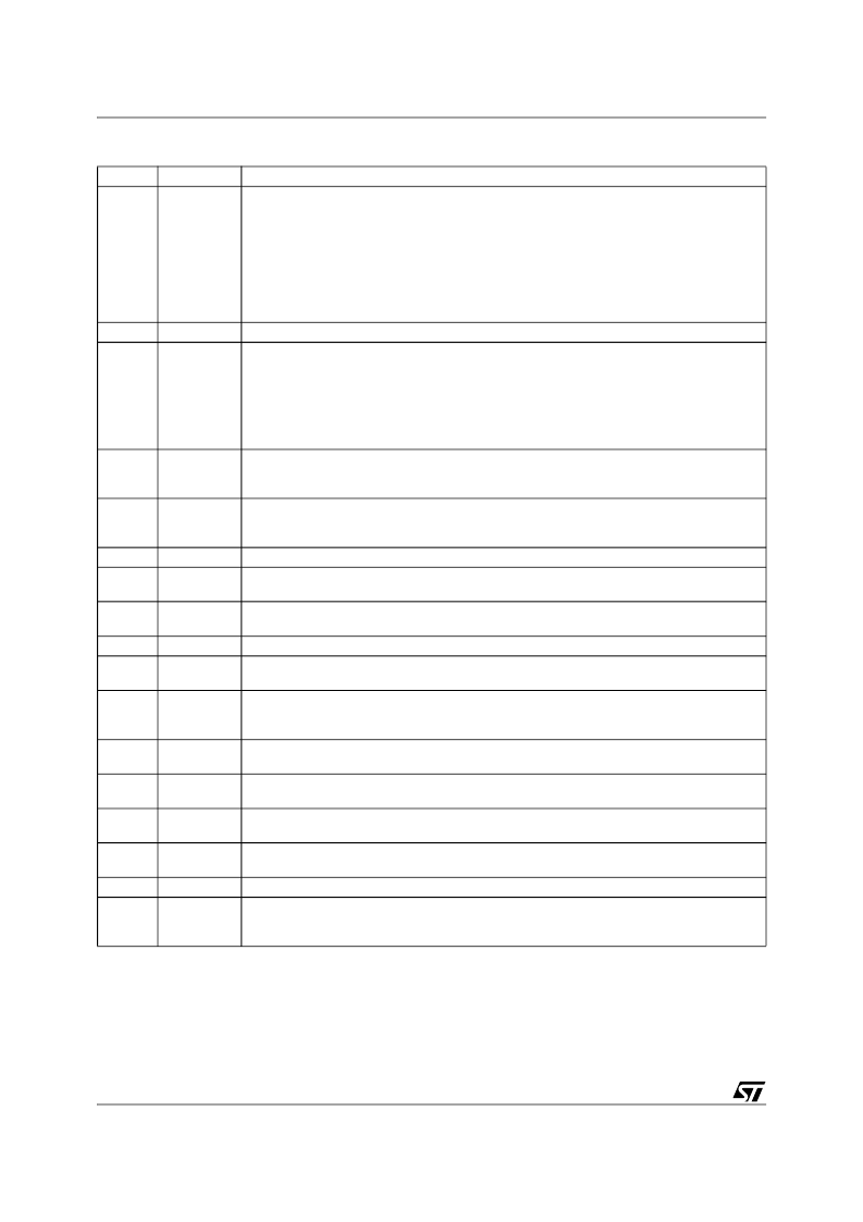
22
OSC/FAULT
Oscillator pin.
It allows programming the switching frequency of each channel: the equivalent switching
frequency at the load side results in being doubled.
Internally fixed at 1.24V, the frequency is varied proportionally to the current sunk (forced)
from (into) the pin with an internal gain of 6kHz/
μ
A (See relevant section for details). If the
pin is not connected, the switching frequency is 150kHz for each channel (300kHz on the
load).
The pin is forced high (5V Typ.) when an Over/Under Voltage is detected; to recover from
these latched conditions, cycle VCC.
Not internally bonded.
Voltage IDentification pins.
Internally pulled-up, connect to SGND to program a ‘0’ while leave floating to program a ‘1’.
They are used to program the output voltage as specified in Table 1 and to set the PGOOD,
OVP and UVP thresholds.
Since the VID pins program the maximum output voltage, according to VRD10 specs, the
device automatically regulates to a voltage VID* = VID–25mV avoiding use of any external
component to lower the regulated voltage.
This pin is an open collector output and is pulled low if the output voltage is not within the
above-specified thresholds and during soft-start. It cannot be pulled up above 3.3V
If not used may be left floating.
Channel 2 HS driver supply. This pin supplies the relative high side driver.
Connect through a capacitor (100nF typ.) to the PHASE2 pin and through a diode to VCC
(cathode vs. boot).
Not internally bonded.
Channel 2 HS driver output.
A little series resistor helps in reducing device-dissipated power.
Channel 2 HS driver return path. It must be connected to the HS2 mosfet source and
provides the return path for the HS driver of channel 2.
Not internally bonded.
Channel 2 LS driver output.
A little series resistor helps in reducing device-dissipated power.
LS drivers return path.
This pin is common to both sections and it must be connected through the closest path to
the LS mosfets source pins in order to reduce the noise injection into the device.
Channel 1 LS driver output.
A little series resistor helps in reducing device-dissipated power.
LS drivers supply: it can be varied from 5V to 12V buses.
Filter locally with at least 1
μ
F ceramic cap vs. PGND.
Channel 1 HS driver return path. It must be connected to the HS1 mosfet source and
provides the return path for the HS driver of channel 1.
Channel 1 HS driver output.
A little series resistor helps in reducing device-dissipated power.
Not internally bonded.
Thermal pad connects the silicon substrate and makes a good thermal contact with the PCB
to dissipate the power necessary to drive external mosfets. Connect to the GND plane with
several vias to improve thermal conduction.
23
N.C.
VID0-5
24 to 29
30
PGOOD
31
BOOT2
32 to 34
35
N.C.
HGATE2
36
PHASE2
37
38
N.C.
LGATE2
39
PGND
40
LGATE1
41
VCCDR
42
PHASE1
43
HGATE1
44
PAD
N.C.
THERMAL
PAD
PIN FUNCTION
(continued)
N
Name
Description
相關(guān)PDF資料 |
PDF描述 |
|---|---|
| L6712A | TWO-PHASE INTERLEAVED DC/DC CONTROLLER |
| L6712AD | TWO-PHASE INTERLEAVED DC/DC CONTROLLER |
| L6712ADTR | TWO-PHASE INTERLEAVED DC/DC CONTROLLER |
| L6712AQ | TWO-PHASE INTERLEAVED DC/DC CONTROLLER |
| L6712AQTR | TWO-PHASE INTERLEAVED DC/DC CONTROLLER |
相關(guān)代理商/技術(shù)參數(shù) |
參數(shù)描述 |
|---|---|
| L6710TR | 功能描述:功率驅(qū)動(dòng)器IC 6-Bit Dual Ph Contlr RoHS:否 制造商:Micrel 產(chǎn)品:MOSFET Gate Drivers 類型:Low Cost High or Low Side MOSFET Driver 上升時(shí)間: 下降時(shí)間: 電源電壓-最大:30 V 電源電壓-最小:2.75 V 電源電流: 最大功率耗散: 最大工作溫度:+ 85 C 安裝風(fēng)格:SMD/SMT 封裝 / 箱體:SOIC-8 封裝:Tube |
| L6711 | 功能描述:DC/DC 開關(guān)控制器 3 PHASE CONTROLLER RoHS:否 制造商:Texas Instruments 輸入電壓:6 V to 100 V 開關(guān)頻率: 輸出電壓:1.215 V to 80 V 輸出電流:3.5 A 輸出端數(shù)量:1 最大工作溫度:+ 125 C 安裝風(fēng)格: 封裝 / 箱體:CPAK |
| L6711_06 | 制造商:STMICROELECTRONICS 制造商全稱:STMicroelectronics 功能描述:3 Phase controller with dynamic VID and selectable DACs |
| L6711TR | 功能描述:DC/DC 開關(guān)控制器 3 PHASE CONTROLLER RoHS:否 制造商:Texas Instruments 輸入電壓:6 V to 100 V 開關(guān)頻率: 輸出電壓:1.215 V to 80 V 輸出電流:3.5 A 輸出端數(shù)量:1 最大工作溫度:+ 125 C 安裝風(fēng)格: 封裝 / 箱體:CPAK |
| L6712 | 制造商:STMICROELECTRONICS 制造商全稱:STMicroelectronics 功能描述:TWO-PHASE INTERLEAVED DC/DC CONTROLLER |
發(fā)布緊急采購(gòu),3分鐘左右您將得到回復(fù)。