- 您現(xiàn)在的位置:買賣IC網(wǎng) > PDF目錄383237 > L6710 (意法半導(dǎo)體) 6 BIT PROGRAMMABLE DUAL-PHASE CONTROLLER WITH DYNAMIC VID MANAGEMENT PDF資料下載
參數(shù)資料
| 型號: | L6710 |
| 廠商: | 意法半導(dǎo)體 |
| 英文描述: | 6 BIT PROGRAMMABLE DUAL-PHASE CONTROLLER WITH DYNAMIC VID MANAGEMENT |
| 中文描述: | 6位可編程雙相與動(dòng)態(tài)VID管理控制器 |
| 文件頁數(shù): | 25/34頁 |
| 文件大?。?/td> | 1610K |
| 代理商: | L6710 |
第1頁第2頁第3頁第4頁第5頁第6頁第7頁第8頁第9頁第10頁第11頁第12頁第13頁第14頁第15頁第16頁第17頁第18頁第19頁第20頁第21頁第22頁第23頁第24頁當(dāng)前第25頁第26頁第27頁第28頁第29頁第30頁第31頁第32頁第33頁第34頁
25/34
L6710
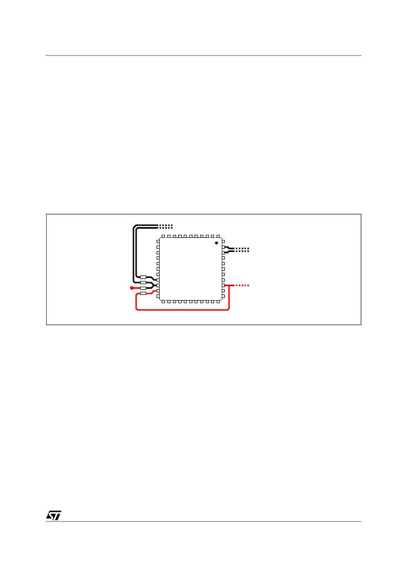
after the pin and connected through Rg to the sense point (see Fig. 17). The PCB traces connecting
these resistors to the reading point must be routed as parallel traces in order to avoid the pick-up of any
common mode noise. It's also important to avoid any offset in the measurement and to get a better pre-
cision, to connect the traces as close as possible to the sensing elements, dedicated current sense re-
sistor or low side mosfet R
dsON
.
Moreover, when using the low side mosfet R
dsON
as current sense element, the ISENx pin is practically
connected to the PHASEx pin. DO NOT CONNECT THE PINS TOGETHER AND THEN TO THE HS
SOURCE! The device won't work properly because of the noise generated by the return of the high side
driver. In this case route two separate nets: connect the PHASEx pin to the HS Source (route together
with HGATEx) with a wide net (30 mils) and the ISENx pin to the LS Drain (route together with PGNDS).
Moreover, the PGNDS pin is always connected, through the Rg resistor, to the PGND: DO NOT CON-
NECT DIRECTLY TO THE PGND! In this case the device won't work properly. Route anyway to the LS
mosfet source (together with ISENx net).
Right and wrong connections are reported in Figure 18.
Symmetrical layout is also suggested to avoid any unbalance between the two phases of the converter.
Figure 18. PCB layout connections for sense nets.
EMBEDDING L6710-BASED VRMs…
When embedding the VRM into the application, additional care must be taken since the whole VRM is a
switching DC/DC regulator and the most common system in which it has to work is a digital system such
as MB or similar. In fact, latest MB has become faster and powerful: high speed data bus are more and
more common and switching-induced noise produced by the VRM can affect data integrity if not following
additional layout guidelines. Few easy points must be considered mainly when routing traces in which
switching high currents flow (switching high currents cause voltage spikes across the stray inductance of
the traces causing noise that can affect the near traces):
– When reproducing high current path on internal layers, please keep all layers the same size in order
to avoid "surrounding" effects that increases noise coupling.
– Keep safe guarding distance between high current switching VRM traces and data buses, especially
if high-speed data bus to minimize noise coupling.
– Keep safe guard distance or filter properly when routing bias traces for I/O sub-systems that must
walk near the VRD.
– Possible causes of noise can be located in the PHASE connections, Mosfet gate drive and Input volt-
age path (from input bulk capacitors and HS drain). Also PGND connections must be considered if
not insisting on a power ground plane. These connections, that can be possible sources of noise,
must be carefully kept far away from noise-sensitive data bus.
To LS Drain and Source
(or Sense Resistor)
To HS Gate and Source
(30 mils wide)
To HS Source
VIA to
GND Plane
NOT CORRECT
CORRECT
相關(guān)PDF資料 |
PDF描述 |
|---|---|
| L6712A | TWO-PHASE INTERLEAVED DC/DC CONTROLLER |
| L6712AD | TWO-PHASE INTERLEAVED DC/DC CONTROLLER |
| L6712ADTR | TWO-PHASE INTERLEAVED DC/DC CONTROLLER |
| L6712AQ | TWO-PHASE INTERLEAVED DC/DC CONTROLLER |
| L6712AQTR | TWO-PHASE INTERLEAVED DC/DC CONTROLLER |
相關(guān)代理商/技術(shù)參數(shù) |
參數(shù)描述 |
|---|---|
| L6710TR | 功能描述:功率驅(qū)動(dòng)器IC 6-Bit Dual Ph Contlr RoHS:否 制造商:Micrel 產(chǎn)品:MOSFET Gate Drivers 類型:Low Cost High or Low Side MOSFET Driver 上升時(shí)間: 下降時(shí)間: 電源電壓-最大:30 V 電源電壓-最小:2.75 V 電源電流: 最大功率耗散: 最大工作溫度:+ 85 C 安裝風(fēng)格:SMD/SMT 封裝 / 箱體:SOIC-8 封裝:Tube |
| L6711 | 功能描述:DC/DC 開關(guān)控制器 3 PHASE CONTROLLER RoHS:否 制造商:Texas Instruments 輸入電壓:6 V to 100 V 開關(guān)頻率: 輸出電壓:1.215 V to 80 V 輸出電流:3.5 A 輸出端數(shù)量:1 最大工作溫度:+ 125 C 安裝風(fēng)格: 封裝 / 箱體:CPAK |
| L6711_06 | 制造商:STMICROELECTRONICS 制造商全稱:STMicroelectronics 功能描述:3 Phase controller with dynamic VID and selectable DACs |
| L6711TR | 功能描述:DC/DC 開關(guān)控制器 3 PHASE CONTROLLER RoHS:否 制造商:Texas Instruments 輸入電壓:6 V to 100 V 開關(guān)頻率: 輸出電壓:1.215 V to 80 V 輸出電流:3.5 A 輸出端數(shù)量:1 最大工作溫度:+ 125 C 安裝風(fēng)格: 封裝 / 箱體:CPAK |
| L6712 | 制造商:STMICROELECTRONICS 制造商全稱:STMicroelectronics 功能描述:TWO-PHASE INTERLEAVED DC/DC CONTROLLER |
發(fā)布緊急采購,3分鐘左右您將得到回復(fù)。