- 您現(xiàn)在的位置:買(mǎi)賣(mài)IC網(wǎng) > PDF目錄373153 > KM4132G271BTQ(R)-10 (SAMSUNG SEMICONDUCTOR CO. LTD.) 128K x 32bit x 2 Banks Synchronous Graphic RAM LVTTL PDF資料下載
參數(shù)資料
| 型號(hào): | KM4132G271BTQ(R)-10 |
| 廠商: | SAMSUNG SEMICONDUCTOR CO. LTD. |
| 英文描述: | 128K x 32bit x 2 Banks Synchronous Graphic RAM LVTTL |
| 中文描述: | 128K的x 32位× 2銀行同步圖形RAM的LVTTL |
| 文件頁(yè)數(shù): | 17/51頁(yè) |
| 文件大?。?/td> | 1033K |
| 代理商: | KM4132G271BTQ(R)-10 |
第1頁(yè)第2頁(yè)第3頁(yè)第4頁(yè)第5頁(yè)第6頁(yè)第7頁(yè)第8頁(yè)第9頁(yè)第10頁(yè)第11頁(yè)第12頁(yè)第13頁(yè)第14頁(yè)第15頁(yè)第16頁(yè)當(dāng)前第17頁(yè)第18頁(yè)第19頁(yè)第20頁(yè)第21頁(yè)第22頁(yè)第23頁(yè)第24頁(yè)第25頁(yè)第26頁(yè)第27頁(yè)第28頁(yè)第29頁(yè)第30頁(yè)第31頁(yè)第32頁(yè)第33頁(yè)第34頁(yè)第35頁(yè)第36頁(yè)第37頁(yè)第38頁(yè)第39頁(yè)第40頁(yè)第41頁(yè)第42頁(yè)第43頁(yè)第44頁(yè)第45頁(yè)第46頁(yè)第47頁(yè)第48頁(yè)第49頁(yè)第50頁(yè)第51頁(yè)

KM4132G271B
CMOS SGRAM
- 17
Rev. 2.4 (May 1998)
WRITE PER BIT
Write per bit(i.e. I/O mask mode) for SGRAM is a function that
selectively masks bits of data being written to the devices. The
mask is stored in an internal register and applied to each bit of
data written when the mask is enabled. Bank active command
with DSF=High enables write per bit for associated bank. Bank
active command with DSF=Low disables write per bit for the
associated bank. The mask used for write per bit operations is
stored in the mask register accessed by SWCBR(Special Mode
Register Set Command). When a mask bit=1, the associated
data bit is written when a write command is executed and write
per bit has been enabled for the bank being written. When a
mask bit=0, the associated data bit is unaltered when a write
command is executed and the write per bit has been enabled for
the bank being written. No additional timing conditions are
required for write per bit operations. Write per bit writes can be
either single write, burst writes or block writes. DQM masking is
the same for write per bit and non-WPB write.
BLOCK WRITE
Block write is a feature allowing the simultaneous writing of
consecutive 8 columns of data within a RAM device during a sin-
gle access cycle. During block write the data to be written comes
from an internal "color" register and DQ I/O pins are used for
independent column selection. The block of column to be written
is aligned on 8 column boundaries and is defined by the column
address with the 3 LSB
′
s ignored. Write command with DSF=1
enables block write for the associated bank. A write command
with DSF=0 enables normal write for the associated bank. The
block width is 8 column where column="n" bits for by "n" part.
The color register is the same width as the data port of the
chip.It is written via a SWCBR where data present on the DQ pin
is to be coupled into the internal color register. The color register
provides the data masked by the DQ column select, WPB
mask(If enabled), and DQM byte mask. Column data mask-
ing(Pixel masking) is provided on an individual column basis for
each byte of data. The column mask is driven on the DQ pins
during a block write command. The DQ column mask function is
segmented on a per bit basis(i.e. DQ[0:7] provides the column
mask for data bits[0:7], DQ[8:15] provides the column mask for
data bits[8:15], DQ0 masks column[0] for data bits[0:7], DQ9
masks column [1] for data bits [8:15], etc). Block writes are
always non-burst, independent of the burst length that has been
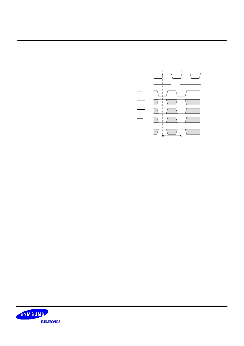
programmed into the mode register. Back to back block writes
are allowed provided that the specified block write cycle
time(
t
BWC
) is satisfied. If write per bit was enabled by the bank
active command with DSF=1, then write per bit masking of the
color register data is enabled.
If write per bit was disabled by a bank active command with
DSF=0, the write per bit masking of the color register data is dis-
abled. DQM masking provides independent data byte masking
during block write exactly the same as it does during normal
write operations, except that the control is extended to the con-
secutive 8 columns of the block write.
DEVICE OPERATIONS (Continued)
1 CLK BW
CLOCK
CKE
CS
RAS
CAS
WE
DSF
HIGH
0
1
2
Timing Diagram to lllustrate
t
BWC
相關(guān)PDF資料 |
PDF描述 |
|---|---|
| KM4132G271BTQ(R)-7 | 128K x 32bit x 2 Banks Synchronous Graphic RAM LVTTL |
| KM4132G271BTQ(R)-8 | 128K x 32bit x 2 Banks Synchronous Graphic RAM LVTTL |
| KM4132G271B | 128K x 32bit x 2 Banks Synchronous Graphic RAM LVTTL |
| KM4132G271BQ(R)-10 | 128K x 32bit x 2 Banks Synchronous Graphic RAM LVTTL |
| KM4132G271BQ(R)-7 | 128K x 32bit x 2 Banks Synchronous Graphic RAM LVTTL |
相關(guān)代理商/技術(shù)參數(shù) |
參數(shù)描述 |
|---|---|
| KM4132G271BTQR-10 | 制造商:SAMSUNG 制造商全稱(chēng):Samsung semiconductor 功能描述:128K x 32bit x 2 Banks Synchronous Graphic RAM LVTTL |
| KM4132G271BTQR-7 | 制造商:SAMSUNG 制造商全稱(chēng):Samsung semiconductor 功能描述:128K x 32bit x 2 Banks Synchronous Graphic RAM LVTTL |
| KM4132G271BTQR-8 | 制造商:SAMSUNG 制造商全稱(chēng):Samsung semiconductor 功能描述:128K x 32bit x 2 Banks Synchronous Graphic RAM LVTTL |
| KM4132G271Q10 | 制造商:SAMSUNG 功能描述:* |
| KM4132G51207 | 制造商:SAMSUNG 功能描述:New |
發(fā)布緊急采購(gòu),3分鐘左右您將得到回復(fù)。