- 您現(xiàn)在的位置:買賣IC網(wǎng) > PDF目錄374297 > K9F4008W0A (SAMSUNG SEMICONDUCTOR CO. LTD.) 512K x 8 bit NAND Flash Memory PDF資料下載
參數(shù)資料
| 型號(hào): | K9F4008W0A |
| 廠商: | SAMSUNG SEMICONDUCTOR CO. LTD. |
| 英文描述: | 512K x 8 bit NAND Flash Memory |
| 中文描述: | 為512k × 8位NAND快閃記憶體 |
| 文件頁數(shù): | 6/24頁 |
| 文件大小: | 318K |
| 代理商: | K9F4008W0A |
K9F4008W0A-TCB0, K9F4008W0A-TIB0
FLASH MEMORY
6
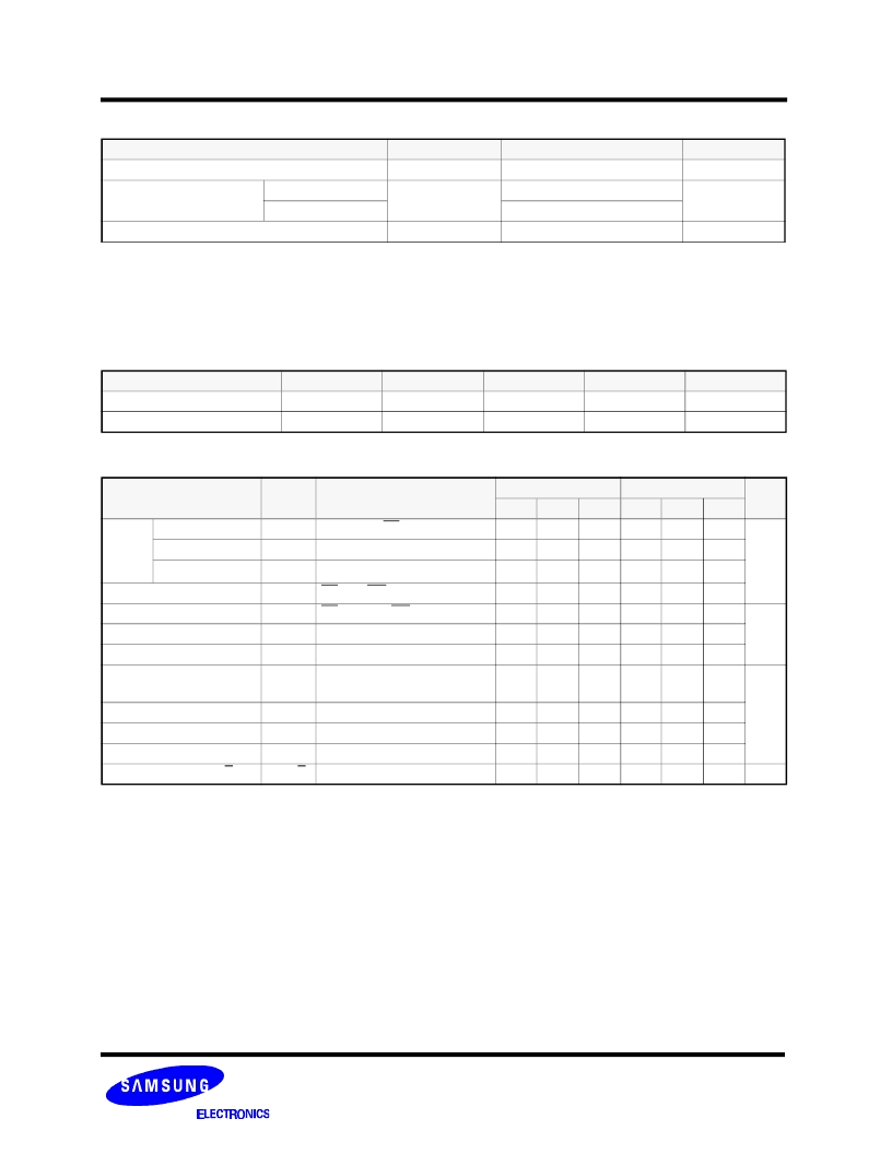
DC AND OPERATING CHARACTERISTICS
(Recommended operating conditions otherwise noted.)
Parameter
Symbol
Test Conditions
Vcc = 3.0V ~ 3.6V
Vcc = 3.6V ~ 5.5V
Unit
Min
Typ
Max
Min
Typ
Max
Oper-
ating
Current
Burst Read Cycle
I
CC1
tRC=120ns,CE=V
IL
, I
OUT
=0mA
-
5
10
-
10
20
mA
Program
I
CC2
-
-
5
10
-
10
20
Erase
I
CC3
-
-
5
10
-
10
20
Stand-by Current(TTL)
I
SB1
CE=V
IH
, WP=0V/V
CC
-
-
1
-
-
1
Stand-by Current(CMOS)
I
SB2
CE=V
CC
-0.2, WP=0V/V
CC
-
10
50
-
10
50
μ
A
Input Leakage Current
I
LI
V
IN
=0 to 5.5V
-
-
±
10
±
10
-
-
±
10
±
10
Output Leakage Current
I
LO
V
OUT
=0 to 5.5V
-
-
-
-
Input High Voltage, All
inputs
V
IH
-
2.4
-
V
CC
+
0.3
2.4
-
V
CC
+
0.5
V
Input Low Voltage, All inputs
V
IL
-
-0.3
-
0.6
-0.3
-
0.8
Output High Voltage Level
V
OH
I
OH
=-400
μ
A
2.4
-
-
2.4
-
-
Output Low Voltage Level
V
OL
I
OL
=2.1mA
-
-
0.4
-
-
0.4
Output Low Current(R/B)
I
OL
(R/B)
V
OL
=0.4V
8
10
-
8
10
-
mA
ABSOLUTE MAXIMUM RATINGS
NOTE
:
1. Minimum DC voltage is -0.6V on input/output pins. During transitions, this level may undershoot to -2.0V for periods <20ns.
Maximum DC voltage on input/output pins is V
CC
+0.3V which, during transitions, may overshoot to V
CC
+2.0V for periods <20ns.
2. Permanent device damage may occur if ABSOLUTE MAXIMUM RATINGS are exceeded. Functional operation should be restricted to the conditions
as detailed in the operational sections of this data sheet. Exposure to absolute maximum rating conditions for extended periods may affect reliability.
Parameter
Symbol
Rating
Unit
Voltage on any pin relative to V
SS
V
IN
-0.6 to +7.0
V
Temperature Under Bias
K9F4008W0A-TCB0
T
BIAS
-10 to +125
°
C
K9F4008W0A-TIB0
-40 to +125
Storage Temperature
T
STG
-65 to +150
°
C
RECOMMENDED OPERATING CONDITIONS
(Voltage reference to GND, K9F4008W0A-TCB0
:
T
A
=0 to 70
°
C, K9F4008W0A-TIB0
:
T
A
=-40 to 85
°
C)
Parameter
Symbol
Min
Typ.
Max
Unit
Supply Voltage
V
CC
3.0
-
5.5
V
Supply Voltage
V
SS
0
0
0
V
相關(guān)PDF資料 |
PDF描述 |
|---|---|
| K9F4008W0A- | 512K x 8 bit NAND Flash Memory |
| K9F4008W0A-TCB0 | Circular Connector; MIL SPEC:MIL-DTL-38999 Series III; Body Material:Metal; Series:TVPS00; No. of Contacts:37; Connector Shell Size:25; Connecting Termination:Crimp; Circular Shell Style:Wall Mount Receptacle; Body Style:Straight |
| K9F4008W0A-TIB0 | Circular Connector; MIL SPEC:MIL-DTL-38999 Series III; Body Material:Metal; Series:TVPS00; No. of Contacts:37; Connector Shell Size:25; Connecting Termination:Crimp; Circular Shell Style:Wall Mount Receptacle; Body Style:Straight |
| K9F4G08U0M | 512M x 8 Bits / 1G x 8 Bits NAND Flash Memory |
| K9K8G08U1M | 512M x 8 Bits / 1G x 8 Bits NAND Flash Memory |
相關(guān)代理商/技術(shù)參數(shù) |
參數(shù)描述 |
|---|---|
| K9F4008W0A- | 制造商:SAMSUNG 制造商全稱:Samsung semiconductor 功能描述:512K x 8 bit NAND Flash Memory |
| K9F4008W0A-TCB0 | 制造商:SAMSUNG 制造商全稱:Samsung semiconductor 功能描述:512K x 8 bit NAND Flash Memory |
| K9F4008W0A-TIB0 | 制造商:SAMSUNG 制造商全稱:Samsung semiconductor 功能描述:512K x 8 bit NAND Flash Memory |
| K9F4G08U0A | 制造商:SAMSUNG 制造商全稱:Samsung semiconductor 功能描述:FLASH MEMORY |
| K9F4G08U0A-I | 制造商:SAMSUNG 制造商全稱:Samsung semiconductor 功能描述:FLASH MEMORY |
發(fā)布緊急采購,3分鐘左右您將得到回復(fù)。