- 您現(xiàn)在的位置:買賣IC網(wǎng) > PDF目錄296206 > IDT72V3640L39268BBGI (INTEGRATED DEVICE TECHNOLOGY INC) 1K X 36 OTHER FIFO, 5 ns, PBGA144 PDF資料下載
參數(shù)資料
| 型號(hào): | IDT72V3640L39268BBGI |
| 廠商: | INTEGRATED DEVICE TECHNOLOGY INC |
| 元件分類: | FIFO |
| 英文描述: | 1K X 36 OTHER FIFO, 5 ns, PBGA144 |
| 封裝: | 13 X 13 MM, 1 MM PITCH, GREEN, PLASTIC, BGA-144 |
| 文件頁數(shù): | 36/46頁 |
| 文件大?。?/td> | 453K |
| 代理商: | IDT72V3640L39268BBGI |
第1頁第2頁第3頁第4頁第5頁第6頁第7頁第8頁第9頁第10頁第11頁第12頁第13頁第14頁第15頁第16頁第17頁第18頁第19頁第20頁第21頁第22頁第23頁第24頁第25頁第26頁第27頁第28頁第29頁第30頁第31頁第32頁第33頁第34頁第35頁當(dāng)前第36頁第37頁第38頁第39頁第40頁第41頁第42頁第43頁第44頁第45頁第46頁
41
COMMERCIAL AND INDUSTRIAL
TEMPERATURE RANGES
IDT72V3640/50/60/70/80/90 3.3V HIGH DENSITY SUPERSYNC IITM 36-BIT FIFO
1,024 x 36, 2,048 x 36, 4,096 x 36, 8,192 x 36, 16,384 x 36 and 32,768 x 36
NOVEMBER 2, 2005
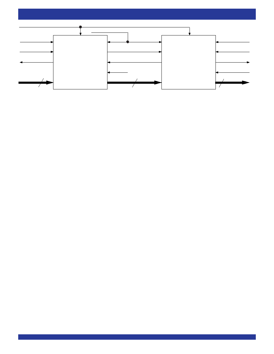
Figure 30. Block Diagram of 2,048 x 36, 4,096 x 36, 8,192 x 36, 16,384 x 36, 32,768 x 36 and 65,536 x 36 Depth Expansion
DEPTH EXPANSION CONFIGURATION (FWFT MODE ONLY)
The IDT72V3640 can easily be adapted to applications requiring depths
greater than 1,024, 2,048 for the IDT72V3650, 4,096 for the IDT72V3660,
8,192 for the IDT72V3670, 16,384 for the IDT72V3680 and 32,768 for the
IDT72V3690 with an 36-bit bus width. In FWFT mode, the FIFOs can be
connected in series (the data outputs of one FIFO connected to the data inputs
of the next) with no external logic necessary. The resulting configuration
provides a total depth equivalent to the sum of the depths associated with each
single FIFO. Figure 30 shows a depth expansion using two IDT72V3640/
72V3650/72V3660/72V3670/72V3680/72V3690 devices.
CareshouldbetakentoselectFWFTmodeduringMasterResetforallFIFOs
in the depth expansion configuration. The first word written to an empty
configuration will pass from one FIFO to the next ("ripple down") until it finally
appears at the outputs of the last FIFO in the chain – no read operation is
necessarybuttheRCLKofeachFIFOmustbefree-running. Eachtimethedata
word appears at the outputs of one FIFO, that device's
OR line goes LOW,
enabling a write to the next FIFO in line.
For an empty expansion configuration, the amount of time it takes for
ORof
the last FIFO in the chain to go LOW (i.e. valid data to appear on the last FIFO's
outputs) after a word has been written to the first FIFO is the sum of the delays
for each individual FIFO:
(N – 1)*(4*transfer clock) + 3*TRCLK
whereNisthenumberofFIFOsintheexpansionandTRCLK istheRCLKperiod.
Note that extra cycles should be added for the possibility that the tSKEW1
specificationisnotmetbetweenWCLKandtransferclock,orRCLKandtransfer
clock, for the
OR flag.
The"rippledown"delayisonlynoticeableforthefirstwordwrittentoanempty
depth expansion configuration. There will be no delay evident for subsequent
words written to the configuration.
The first free location created by reading from a full depth expansion
configurationwill"bubbleup"fromthelastFIFOtothepreviousoneuntilitfinally
movesintothefirstFIFOofthechain. Eachtimeafreelocationiscreatedinone
FIFO of the chain, that FIFO's
IRlinegoesLOW,enablingtheprecedingFIFO
to write a word to fill it.
Forafullexpansionconfiguration,theamountoftimeittakesfor
IRofthefirst
FIFO in the chain to go LOW after a word has been read from the last FIFO is
the sum of the delays for each individual FIFO:
(N – 1)*(3*transfer clock) + 2 TWCLK
where N is the number of FIFOs in the expansion and TWCLK is the WCLK
period. NotethatextracyclesshouldbeaddedforthepossibilitythatthetSKEW1
specificationisnotmetbetweenRCLKandtransferclock,orWCLKandtransfer
clock, for the
IR flag.
The Transfer Clock line should be tied to either WCLK or RCLK, whichever
isfaster. Boththeseactionsresultindatamoving,asquicklyaspossible,tothe
end of the chain and free locations to the beginning of the chain.
Dn
INPUT READY
WRITE ENABLE
WRITE CLOCK
WEN
WCLK
IR
DATA IN
RCLK
READ CLOCK
RCLK
REN
OE
OUTPUT ENABLE
OUTPUT READY
Qn
Dn
IR
GND
WEN
WCLK
OR
REN
OE
Qn
READ ENABLE
OR
DATA OUT
IDT
72V3640
72V3650
72V3660
72V3670
72V3680
72V3690
TRANSFER CLOCK
4667 drw 35
n
FWFT/SI
IDT
72V3640
72V3650
72V3660
72V3670
72V3680
72V3690
相關(guān)PDF資料 |
PDF描述 |
|---|---|
| IDT79R4600-133MD | 64-BIT, 133 MHz, RISC PROCESSOR, PQFP208 |
| IDT79RV4400SC-67GL447 | 64-BIT, 67 MHz, RISC PROCESSOR, CPGA447 |
| IDT79RV4400SC-100GL447 | 64-BIT, 100 MHz, RISC PROCESSOR, CPGA447 |
| IDT7M7004S75CH | 128K X 8 EEPROM 5V MODULE, 75 ns, CPGA66 |
| IFD010P2SAXXXXX | 5 Mbps, IDE COMPATIBLE, FLASH MEMORY DRIVE CONTROLLER, XMA68 |
相關(guān)代理商/技術(shù)參數(shù) |
參數(shù)描述 |
|---|---|
| IDT72V3640L6BB | 功能描述:IC FIFO SS 1024X36 6NS 144-BGA RoHS:否 類別:集成電路 (IC) >> 邏輯 - FIFO 系列:72V 標(biāo)準(zhǔn)包裝:90 系列:7200 功能:同步 存儲(chǔ)容量:288K(16K x 18) 數(shù)據(jù)速率:100MHz 訪問時(shí)間:10ns 電源電壓:4.5 V ~ 5.5 V 工作溫度:0°C ~ 70°C 安裝類型:表面貼裝 封裝/外殼:64-LQFP 供應(yīng)商設(shè)備封裝:64-TQFP(14x14) 包裝:托盤 其它名稱:72271LA10PF |
| IDT72V3640L6BB8 | 功能描述:IC FIFO SS 1024X36 6NS 144-BGA RoHS:否 類別:集成電路 (IC) >> 邏輯 - FIFO 系列:72V 標(biāo)準(zhǔn)包裝:90 系列:7200 功能:同步 存儲(chǔ)容量:288K(16K x 18) 數(shù)據(jù)速率:100MHz 訪問時(shí)間:10ns 電源電壓:4.5 V ~ 5.5 V 工作溫度:0°C ~ 70°C 安裝類型:表面貼裝 封裝/外殼:64-LQFP 供應(yīng)商設(shè)備封裝:64-TQFP(14x14) 包裝:托盤 其它名稱:72271LA10PF |
| IDT72V3640L6BBG | 制造商:Integrated Device Technology Inc 功能描述:FIFO Mem Sync Dual Depth/Width Uni-Dir 1K x 36 144-Pin BGA |
| IDT72V3640L6PF | 功能描述:IC FIFO SS 1024X36 6NS 128-TQFP RoHS:否 類別:集成電路 (IC) >> 邏輯 - FIFO 系列:72V 標(biāo)準(zhǔn)包裝:90 系列:7200 功能:同步 存儲(chǔ)容量:288K(16K x 18) 數(shù)據(jù)速率:100MHz 訪問時(shí)間:10ns 電源電壓:4.5 V ~ 5.5 V 工作溫度:0°C ~ 70°C 安裝類型:表面貼裝 封裝/外殼:64-LQFP 供應(yīng)商設(shè)備封裝:64-TQFP(14x14) 包裝:托盤 其它名稱:72271LA10PF |
| IDT72V3640L6PF8 | 功能描述:IC FIFO SS 1024X36 6NS 128-TQFP RoHS:否 類別:集成電路 (IC) >> 邏輯 - FIFO 系列:72V 標(biāo)準(zhǔn)包裝:90 系列:7200 功能:同步 存儲(chǔ)容量:288K(16K x 18) 數(shù)據(jù)速率:100MHz 訪問時(shí)間:10ns 電源電壓:4.5 V ~ 5.5 V 工作溫度:0°C ~ 70°C 安裝類型:表面貼裝 封裝/外殼:64-LQFP 供應(yīng)商設(shè)備封裝:64-TQFP(14x14) 包裝:托盤 其它名稱:72271LA10PF |
發(fā)布緊急采購,3分鐘左右您將得到回復(fù)。