- 您現(xiàn)在的位置:買賣IC網(wǎng) > PDF目錄67710 > ICSSSTUF32866EHLFT (INTEGRATED DEVICE TECHNOLOGY INC) SSTU SERIES, POSITIVE EDGE TRIGGERED D FLIP-FLOP, TRUE OUTPUT, PBGA96 PDF資料下載
參數(shù)資料
| 型號: | ICSSSTUF32866EHLFT |
| 廠商: | INTEGRATED DEVICE TECHNOLOGY INC |
| 元件分類: | 鎖存器 |
| 英文描述: | SSTU SERIES, POSITIVE EDGE TRIGGERED D FLIP-FLOP, TRUE OUTPUT, PBGA96 |
| 封裝: | GREEN, MO-205CC, LFBGA-96 |
| 文件頁數(shù): | 2/27頁 |
| 文件大?。?/td> | 310K |
| 代理商: | ICSSSTUF32866EHLFT |
第1頁當(dāng)前第2頁第3頁第4頁第5頁第6頁第7頁第8頁第9頁第10頁第11頁第12頁第13頁第14頁第15頁第16頁第17頁第18頁第19頁第20頁第21頁第22頁第23頁第24頁第25頁第26頁第27頁
10
ICSSSTUF32866E
1038B—05/03/05
CK
D1D25
RST#
tsu
tpd
CK to PPO
th
tsu
th
tpdm , t pdmss
CK to Q
DCS#
CSR#
CK#
Q1Q25
PAR_IN
n
n + 1
n + 2
PPO
n + 3
n + 4
tPHL
CK to QERR#
QERR#
tPHL , t PLH
CK to QERR#
tact
H, L, or X
H or L
Data to QERR# Latency
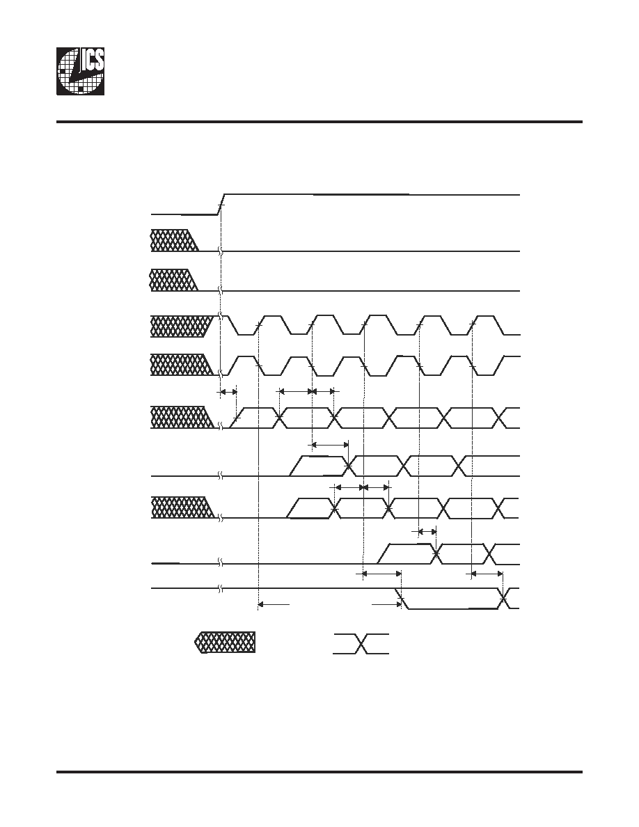
Figure 9 — Timing diagram for SSTU32866 used as a single device; C0=0, C1=0;
RST# Switches from L to H
After RST# is switched from low to high, all data and PAR_IN inputs signals must be set and held low for a minimum time of t
max, to avoid false error.
If the data is clocked in on the n clock pulse, the QERR# output signal will be generated on the n+2 clock pulse, and it will be valid on
the n+3 clock pulse.
ACT
2. Device standard (cont'd)
2.7 Register timing
相關(guān)PDF資料 |
PDF描述 |
|---|---|
| ICSSSTVA16859CK-LF | SSTV SERIES, POSITIVE EDGE TRIGGERED D FLIP-FLOP, TRUE OUTPUT, QCC56 |
| ICSSSTVA16859CK | SSTV SERIES, POSITIVE EDGE TRIGGERED D FLIP-FLOP, TRUE OUTPUT, QCC56 |
| ICSSSTVA16859CGLF-T | SSTV SERIES, POSITIVE EDGE TRIGGERED D FLIP-FLOP, TRUE OUTPUT, PDSO64 |
| ICSSSTVA16859CKLF | SSTV SERIES, POSITIVE EDGE TRIGGERED D FLIP-FLOP, TRUE OUTPUT, QCC56 |
| ICSSTV16859BG-T | SSTV SERIES, POSITIVE EDGE TRIGGERED D FLIP-FLOP, TRUE OUTPUT, PDSO64 |
相關(guān)代理商/技術(shù)參數(shù) |
參數(shù)描述 |
|---|---|
| ICSSSTV16857 | 制造商:ICS 制造商全稱:ICS 功能描述:DDR 14-Bit Registered Buffer |
| ICSSSTV16857CG-T | 制造商:ICS 制造商全稱:ICS 功能描述:DDR 14-Bit Registered Buffer |
| ICSSSTV16857YG-T | 制造商:ICS 制造商全稱:ICS 功能描述:DDR 14-Bit Registered Buffer |
| ICSSSTV16857YL-T | 制造商:ICS 制造商全稱:ICS 功能描述:DDR 14-Bit Registered Buffer |
| ICSSSTV16859 | 制造商:ICS 制造商全稱:ICS 功能描述:DDR 13-Bit to 26-Bit Registered Buffer |
發(fā)布緊急采購,3分鐘左右您將得到回復(fù)。