- 您現(xiàn)在的位置:買賣IC網(wǎng) > PDF目錄370795 > HYE25L256160AC-8 (INFINEON TECHNOLOGIES AG) 256-Mbit Mobile-RAM PDF資料下載
參數(shù)資料
| 型號: | HYE25L256160AC-8 |
| 廠商: | INFINEON TECHNOLOGIES AG |
| 英文描述: | 256-Mbit Mobile-RAM |
| 中文描述: | 256兆移動RAM |
| 文件頁數(shù): | 7/55頁 |
| 文件大?。?/td> | 1053K |
| 代理商: | HYE25L256160AC-8 |
第1頁第2頁第3頁第4頁第5頁第6頁當(dāng)前第7頁第8頁第9頁第10頁第11頁第12頁第13頁第14頁第15頁第16頁第17頁第18頁第19頁第20頁第21頁第22頁第23頁第24頁第25頁第26頁第27頁第28頁第29頁第30頁第31頁第32頁第33頁第34頁第35頁第36頁第37頁第38頁第39頁第40頁第41頁第42頁第43頁第44頁第45頁第46頁第47頁第48頁第49頁第50頁第51頁第52頁第53頁第54頁第55頁
Data Sheet
7
V1.1, 2003-04-16
HYE25L256160AC
256-Mbit Mobile-RAM
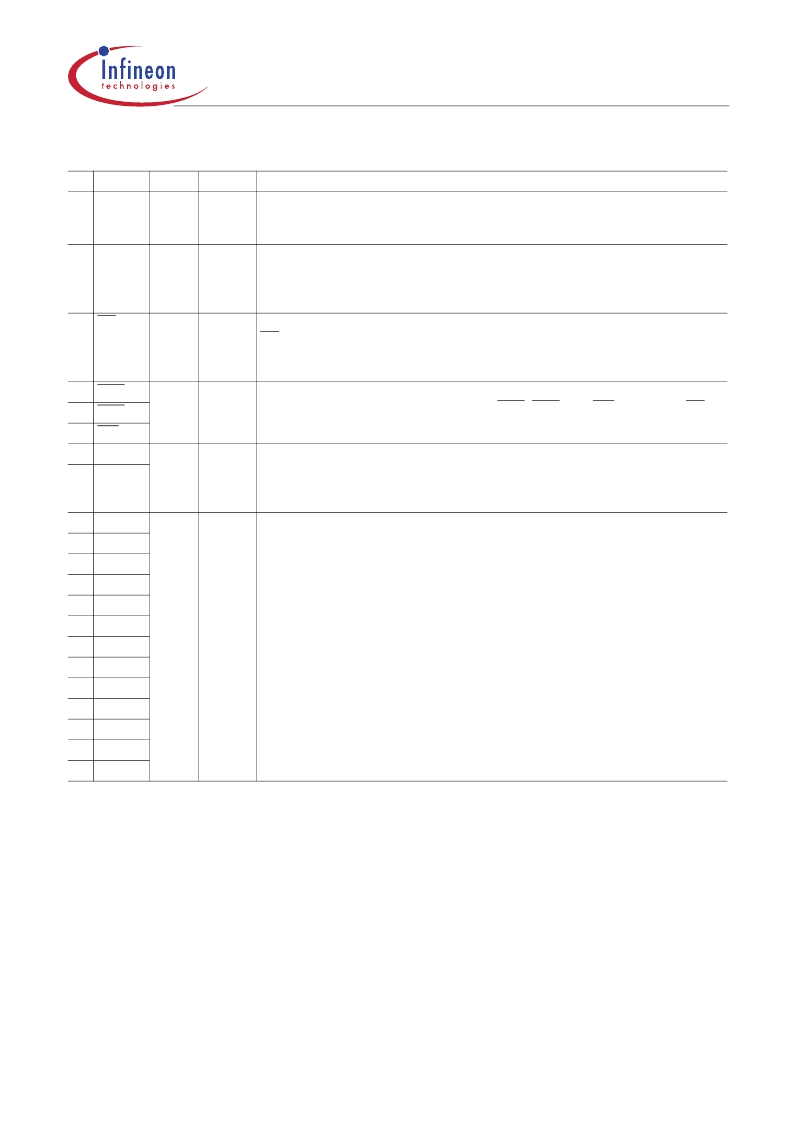
Pin Configuration
Table 3
Pin Symbol Type
F2
CLK
Input/Output Signals
Polarity Function
Input
Positive
Edge
Clock
The system clock input. All of the SDRAM inputs are sampled on the rising edge
of the clock.
Clock Enable
CKE activates the CLK signal when high and deactivates the CLK signal when
low, thereby initiates either the Power Down mode, Suspend mode, or the Self
Refresh mode.
Chip Select
CS enables the command decoder when low and disables the command
decoder when high. When the command decoder is disabled, new commands
are ignored but previous operations continue.
Command Inputs
Sampled at the rising edge of the clock, RAS, CAS, and WE (along with CS)
define the command to be executed by the SDRAM.
F3
CKE
Input
Active
High
G9 CS
Input
Active
Low
F8
F7
F9
G8 BA1
G7 BA0
RAS
CAS
WE
Input
Active
Low
Input
Active
High
Bank Address Inputs
BA0 and BA1 define to which bank an Active, Read, Write or Precharge
command is being applied. BA0 and BA1 also determine if the mode register or
extended mode register is to be accessed during a MRS or EMRS cycle.
Address Inputs
During a Bank Activate command cycle, A12 - A0 define the row address
(RA12 - RA0) when sampled at the rising clock edge.
During a Read or Write command cycle, A8-A0 define the column address
(CA8 - CA0) when sampled at the rising clock edge.
In addition to the column address, A10/AP is used to invoke autoprecharge
operation at the end of the burst read or write cycle. If AP is high, autoprecharge
is selected and BA1, BA0 defines the bank to be precharged. If AP is low,
autoprecharge is disabled.
During a Precharge command cycle, AP is used in conjunction with BA1 and
BA0 to control which bank(s) to precharge. If AP is high, all four banks will be
precharged regardless of the state of BA0 and BA1. If AP is low, then BA1 and
BA0 are used to define which bank to precharge.
G1 A12
G2 A11
H9
G3 A9
H1
H2
H3
J2
J3
J7
J8
H8
H7
Input
Active
High
A10/AP
A8
A7
A6
A5
A4
A3
A2
A1
A0
相關(guān)PDF資料 |
PDF描述 |
|---|---|
| HYE25L256160AF | 256MBit Mobile-RAM |
| HYE25L256160AF-75 | CAP TANT 10UF 6.3V 20% SMD |
| HYE25L256160AC-7.5 | BJAWBMSpecialty DRAMs Mobile-RAM |
| HYM321000GS-60 | 1M x 32-Bit Dynamic RAM Module 2M x 16-Bit Dynamic RAM Module |
| HYM321000S-60 | 1M x 32-Bit Dynamic RAM Module 2M x 16-Bit Dynamic RAM Module |
相關(guān)代理商/技術(shù)參數(shù) |
參數(shù)描述 |
|---|---|
| HYE25L256160AF | 制造商:INFINEON 制造商全稱:Infineon Technologies AG 功能描述:256MBit Mobile-RAM |
| HYE25L256160AF-7.5 | 制造商:INFINEON 制造商全稱:Infineon Technologies AG 功能描述:BJAWBMSpecialty DRAMs Mobile-RAM |
| HYE25L256160AF-75 | 制造商:INFINEON 制造商全稱:Infineon Technologies AG 功能描述:256MBit Mobile-RAM |
| HYESD0514P | 制造商:HY 制造商全稱:HY ELECTRONIC CORP. 功能描述:4 Channel Low Capacitance ESD Protection Diode Array |
發(fā)布緊急采購,3分鐘左右您將得到回復(fù)。