- 您現(xiàn)在的位置:買賣IC網(wǎng) > PDF目錄296198 > HY5DU12422BLT-H (HYNIX SEMICONDUCTOR INC) 128M X 4 DDR DRAM, 0.75 ns, PDSO66 PDF資料下載
參數(shù)資料
| 型號(hào): | HY5DU12422BLT-H |
| 廠商: | HYNIX SEMICONDUCTOR INC |
| 元件分類: | DRAM |
| 英文描述: | 128M X 4 DDR DRAM, 0.75 ns, PDSO66 |
| 封裝: | 0.400 X 0.875 INCH, 0.65 MM PITCH, TSOP2-66 |
| 文件頁(yè)數(shù): | 10/31頁(yè) |
| 文件大小: | 686K |
| 代理商: | HY5DU12422BLT-H |
第1頁(yè)第2頁(yè)第3頁(yè)第4頁(yè)第5頁(yè)第6頁(yè)第7頁(yè)第8頁(yè)第9頁(yè)當(dāng)前第10頁(yè)第11頁(yè)第12頁(yè)第13頁(yè)第14頁(yè)第15頁(yè)第16頁(yè)第17頁(yè)第18頁(yè)第19頁(yè)第20頁(yè)第21頁(yè)第22頁(yè)第23頁(yè)第24頁(yè)第25頁(yè)第26頁(yè)第27頁(yè)第28頁(yè)第29頁(yè)第30頁(yè)第31頁(yè)
Rev. 1.1 / Apr. 2006
18
1HY5DU12422B(L)T
HY5DU12822B(L)T
HY5DU121622B(L)T
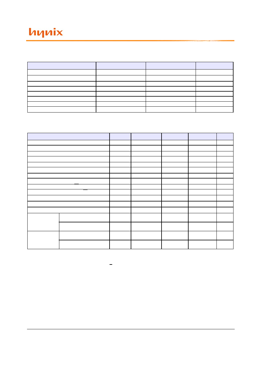
ABSOLUTE MAXIMUM RATINGS
Note: Operation at above absolute maximum rating can adversely affect device reliability
DC OPERATING CONDITIONS (TA=0 to 70 oC, Voltage referenced to VSS = 0V)
Note:
1. VDDQ must not exceed the level of VDD.
2. VIL (min) is acceptable -1.5V AC pulse width with < 5ns of duration.
3. VREF is expected to be equal to 0.5*VDDQ of the transmitting device, and to track variations in the dc level of the same.
Peak to peak noise on VREF may not exceed ± 2% of the DC value.
4. VID is the magnitude of the difference between the input level on CK and the input level on /CK.
5. The ratio of the pullup current to the pulldown current is specified for the same temperature and voltage, over the entire temper-
ature and voltage range, for device drain to source voltages from 0.25V to 1.0V. For a given output, it represents the maximum dif-
ference between pullup and pulldown drivers due to process variation. The full variation in the ratio of the maximum to minimum
pullup and pulldown current will not exceed 1/7 for device drain to source voltages from 0.1 to 1.0.
6. VIN=0 to VDD, All other pins are not tested under VIN = 0V.
7. DQs are disabled, VOUT=0 to VDDQ
Parameter
Symbol
Rating
Unit
Operating Temperature (Ambient)
TA
0 ~ 70
oC
Storage Temperature
TSTG
-55 ~ 150
oC
Voltage on VDD relative to VSS
VDD
-1.0 ~ 3.6
V
Voltage on VDDQ relative to VSS
VDDQ
-1.0 ~ 3.6
V
Voltage on inputs relative to VSS
VINPUT
-1.0 ~ 3.6
V
Voltage on I/O pins relative to VSS
VIO
-0.5 ~3.6
V
Output Short Circuit Current
IOS
50
mA
Soldering Temperature
Time
TSOLDER
260
10
oC Sec
Parameter
Symbol
Min
Typ.
Max
Unit
Power Supply Voltage (DDR200, 266, 333)
VDD
2.3
2.5
2.7
V
Power Supply Voltage (DDR200, 266, 333)1
VDDQ
2.3
2.5
2.7
V
Power Supply Voltage (DDR400)
VDD
2.5
2.6
2.7
V
Power Supply Voltage (DDR400)1
VDDQ
2.5
2.6
2.7
V
Input High Voltage
VIH
VREF + 0.15
-
VDDQ + 0.3
V
Input Low Voltage2
VIL
-0.3
-
VREF - 0.15
V
Termination Voltage
VTT
VREF - 0.04
VREF
VREF + 0.04
V
Reference Voltage3
VREF
0.49*VDDQ
0.5*VDDQ
0.51*VDDQ
V
Input Voltage Level, CK and CK inputs
VIN(DC)
-0.3
-
VDDQ+0.3
V
Input Differential Voltage, CK and CK inputs4
VID(DC)
0.36
-
VDDQ+0.6
V
V-I Matching: Pullup to Pulldown Current Ratio5
VI(RATIO)
0.71
-
1.4
-
Input Leakage Current6
ILI
-2
-
2
uA
Output Leakage Current7
ILO
-5
-
5
uA
Normal Strength
Output Driver
(VOUT=VTT ±0.84)
Output High Current
(min VDDQ, min VREF, min VTT)
IOH
-16.8
-
mA
Output Low Current
(min VDDQ, max VREF, max VTT)
IOL
16.8
-
mA
Half Strength
Output Driver
(VOUT=VTT ±0.68)
Output High Current
(min VDDQ, min VREF, min VTT)
IOH
-13.6
-
mA
Output Low Current
(min VDDQ, max VREF, max VTT)
IOL
13.6
-
mA
相關(guān)PDF資料 |
PDF描述 |
|---|---|
| HY86-12LF | 90-Degree Hybrid 0.82-0.90 GHz |
| HYB25D128400CT-5 | 32M X 4 DDR DRAM, 0.7 ns, PDSO66 |
| HYB25D256160CC-5 | 256 Mbit Double Data Rate SDRAM |
| HYB25S256160AC-7.5 | 16M X 16 SYNCHRONOUS DRAM, 7.5 ns, PBGA54 |
| HYB39S128160TEL-37 | MEMORY SPECTRUM |
相關(guān)代理商/技術(shù)參數(shù) |
參數(shù)描述 |
|---|---|
| HY5DU12422BLTP | 制造商:HYNIX 制造商全稱:Hynix Semiconductor 功能描述:512Mb DDR SDRAM |
| HY5DU12422BLTP-X | 制造商:HYNIX 制造商全稱:Hynix Semiconductor 功能描述:512Mb DDR SDRAM |
| HY5DU12422BT | 制造商:HYNIX 制造商全稱:Hynix Semiconductor 功能描述:512Mb DDR SDRAM |
| HY5DU12422BT_06 | 制造商:HYNIX 制造商全稱:Hynix Semiconductor 功能描述:512Mb DDR SDRAM |
| HY5DU12422BT-H-A | 制造商:Hynix Semi 功能描述: |
發(fā)布緊急采購(gòu),3分鐘左右您將得到回復(fù)。