- 您現(xiàn)在的位置:買賣IC網(wǎng) > PDF目錄368255 > PSD835F2V-C-70U (意法半導(dǎo)體) Configurable Memory System on a Chip for 8-Bit Microcontrollers PDF資料下載
參數(shù)資料
| 型號(hào): | PSD835F2V-C-70U |
| 廠商: | 意法半導(dǎo)體 |
| 英文描述: | Configurable Memory System on a Chip for 8-Bit Microcontrollers |
| 中文描述: | 在8片位微控制器可配置存儲(chǔ)系統(tǒng) |
| 文件頁(yè)數(shù): | 8/110頁(yè) |
| 文件大?。?/td> | 570K |
| 代理商: | PSD835F2V-C-70U |
第1頁(yè)第2頁(yè)第3頁(yè)第4頁(yè)第5頁(yè)第6頁(yè)第7頁(yè)當(dāng)前第8頁(yè)第9頁(yè)第10頁(yè)第11頁(yè)第12頁(yè)第13頁(yè)第14頁(yè)第15頁(yè)第16頁(yè)第17頁(yè)第18頁(yè)第19頁(yè)第20頁(yè)第21頁(yè)第22頁(yè)第23頁(yè)第24頁(yè)第25頁(yè)第26頁(yè)第27頁(yè)第28頁(yè)第29頁(yè)第30頁(yè)第31頁(yè)第32頁(yè)第33頁(yè)第34頁(yè)第35頁(yè)第36頁(yè)第37頁(yè)第38頁(yè)第39頁(yè)第40頁(yè)第41頁(yè)第42頁(yè)第43頁(yè)第44頁(yè)第45頁(yè)第46頁(yè)第47頁(yè)第48頁(yè)第49頁(yè)第50頁(yè)第51頁(yè)第52頁(yè)第53頁(yè)第54頁(yè)第55頁(yè)第56頁(yè)第57頁(yè)第58頁(yè)第59頁(yè)第60頁(yè)第61頁(yè)第62頁(yè)第63頁(yè)第64頁(yè)第65頁(yè)第66頁(yè)第67頁(yè)第68頁(yè)第69頁(yè)第70頁(yè)第71頁(yè)第72頁(yè)第73頁(yè)第74頁(yè)第75頁(yè)第76頁(yè)第77頁(yè)第78頁(yè)第79頁(yè)第80頁(yè)第81頁(yè)第82頁(yè)第83頁(yè)第84頁(yè)第85頁(yè)第86頁(yè)第87頁(yè)第88頁(yè)第89頁(yè)第90頁(yè)第91頁(yè)第92頁(yè)第93頁(yè)第94頁(yè)第95頁(yè)第96頁(yè)第97頁(yè)第98頁(yè)第99頁(yè)第100頁(yè)第101頁(yè)第102頁(yè)第103頁(yè)第104頁(yè)第105頁(yè)第106頁(yè)第107頁(yè)第108頁(yè)第109頁(yè)第110頁(yè)
PSD835G2
PSD8XX Family
7
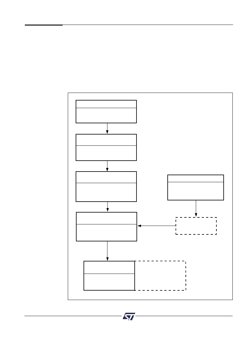
Define General Purpose
Logic in CPLD
Merge MCU Firmware
with PSD Configuration
ST
PSD Programmer
*.OBJ FILE
Point and click definition of
combinatorial and registered logic
in CPLD. Access to HDL is
available if needed.
Define PSD Pin and
Node functions
Point and click definition of
PSD pin functions, internal nodes,
and MCU system memory map.
Choose MCU and PSD
Automatically Configures MCU
bus interface and other PSD
attributes.
PSDPro or
FlashLink (JTAG)
A composite object file is created
containing MCU firmware and
PSD configuration.
C Code Generation
Generate C Code
Specific to PSD
Finctions
User's choice of
Microcontroller
Compiler/Linker
*.OBJ file
available
for 3rd party
programmers
(Conventional or JTAG-ISP)
MCU Firmware
Hex or S-Record
format
Figure 2. PSDsoft Development Tool
5.0
Development
System
The PSD8XX series is supported by PSDsoft a Windows-based (95, 98, NT) software
development tool. A PSD design is quickly and easily produced in a point and click
environment. The designer does not need to enter Hardware Definition Language (HDL)
equations (unless desired) to define PSD pin functions and memory map information. The
general design flow is shown in Figure 2 below. PSDsoft is available from our web site
(www.
st.
com
/psm
) or other distribution channels.
PSDsoft directly supports two low cost device programmers from
ST.
PSDpro
and FlashLINK (JTAG). Both of these programmers may be purchased through your local
rep/distributor, or directly from our web site using a credit card. The PSD8XX is also
supported by third party device programmers, see web site for current list.
相關(guān)PDF資料 |
PDF描述 |
|---|---|
| PSD835F2V-C-70UI | Configurable Memory System on a Chip for 8-Bit Microcontrollers |
| PSD835F2V-C-90B81 | Configurable Memory System on a Chip for 8-Bit Microcontrollers |
| PSD835F2V-C-90B81I | Configurable Memory System on a Chip for 8-Bit Microcontrollers |
| PSD835F2V-C-90J | Configurable Memory System on a Chip for 8-Bit Microcontrollers |
| PSD835F2V-C-90JI | Configurable Memory System on a Chip for 8-Bit Microcontrollers |
相關(guān)代理商/技術(shù)參數(shù) |
參數(shù)描述 |
|---|---|
| PSD835G2-70U | 功能描述:靜態(tài)隨機(jī)存取存儲(chǔ)器 5.0V 4M 70ns RoHS:否 制造商:Cypress Semiconductor 存儲(chǔ)容量:16 Mbit 組織:1 M x 16 訪問時(shí)間:55 ns 電源電壓-最大:3.6 V 電源電壓-最小:2.2 V 最大工作電流:22 uA 最大工作溫度:+ 85 C 最小工作溫度:- 40 C 安裝風(fēng)格:SMD/SMT 封裝 / 箱體:TSOP-48 封裝:Tray |
| PSD835G2-90U | 功能描述:靜態(tài)隨機(jī)存取存儲(chǔ)器 5.0V 4M 90ns RoHS:否 制造商:Cypress Semiconductor 存儲(chǔ)容量:16 Mbit 組織:1 M x 16 訪問時(shí)間:55 ns 電源電壓-最大:3.6 V 電源電壓-最小:2.2 V 最大工作電流:22 uA 最大工作溫度:+ 85 C 最小工作溫度:- 40 C 安裝風(fēng)格:SMD/SMT 封裝 / 箱體:TSOP-48 封裝:Tray |
| PSD835G2-90UI | 功能描述:靜態(tài)隨機(jī)存取存儲(chǔ)器 5.0V 4M 90ns RoHS:否 制造商:Cypress Semiconductor 存儲(chǔ)容量:16 Mbit 組織:1 M x 16 訪問時(shí)間:55 ns 電源電壓-最大:3.6 V 電源電壓-最小:2.2 V 最大工作電流:22 uA 最大工作溫度:+ 85 C 最小工作溫度:- 40 C 安裝風(fēng)格:SMD/SMT 封裝 / 箱體:TSOP-48 封裝:Tray |
| PSD835G2V-12UI | 功能描述:靜態(tài)隨機(jī)存取存儲(chǔ)器 3.0V 4M 120ns RoHS:否 制造商:Cypress Semiconductor 存儲(chǔ)容量:16 Mbit 組織:1 M x 16 訪問時(shí)間:55 ns 電源電壓-最大:3.6 V 電源電壓-最小:2.2 V 最大工作電流:22 uA 最大工作溫度:+ 85 C 最小工作溫度:- 40 C 安裝風(fēng)格:SMD/SMT 封裝 / 箱體:TSOP-48 封裝:Tray |
| PSD835G2V-90U | 功能描述:靜態(tài)隨機(jī)存取存儲(chǔ)器 3.0V 4M 90ns RoHS:否 制造商:Cypress Semiconductor 存儲(chǔ)容量:16 Mbit 組織:1 M x 16 訪問時(shí)間:55 ns 電源電壓-最大:3.6 V 電源電壓-最小:2.2 V 最大工作電流:22 uA 最大工作溫度:+ 85 C 最小工作溫度:- 40 C 安裝風(fēng)格:SMD/SMT 封裝 / 箱體:TSOP-48 封裝:Tray |
發(fā)布緊急采購(gòu),3分鐘左右您將得到回復(fù)。