- 您現(xiàn)在的位置:買賣IC網(wǎng) > PDF目錄296194 > HPC46100 (National Semiconductor Corporation) HPC46100 High-Performance microController with DSP Capability PDF資料下載
參數(shù)資料
| 型號: | HPC46100 |
| 廠商: | National Semiconductor Corporation |
| 英文描述: | HPC46100 High-Performance microController with DSP Capability |
| 中文描述: | HPC46100高性能微控制器與DSP處理能力 |
| 文件頁數(shù): | 4/32頁 |
| 文件大?。?/td> | 436K |
| 代理商: | HPC46100 |
第1頁第2頁第3頁當前第4頁第5頁第6頁第7頁第8頁第9頁第10頁第11頁第12頁第13頁第14頁第15頁第16頁第17頁第18頁第19頁第20頁第21頁第22頁第23頁第24頁第25頁第26頁第27頁第28頁第29頁第30頁第31頁第32頁
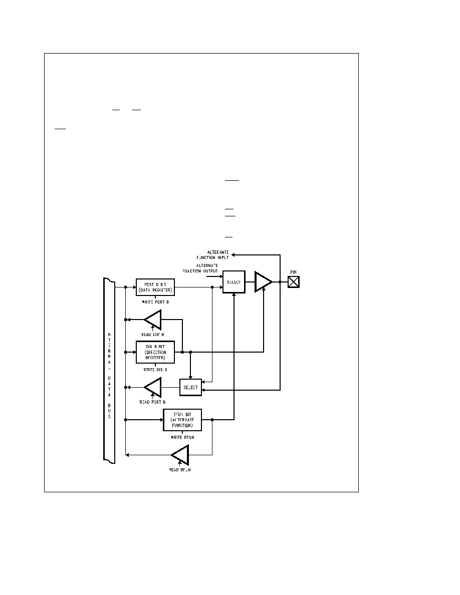
IO Ports
PORT A
Port A is a 16-bit multiplexed addressdata bus used for
accessing external program and data memory Four associ-
ated bus control signals are available on port B The Ad-
dress Latch Enable (ALE) signal is used to provide timing to
demultiplex the bus Reading from and writing to external
memory are signalled by RD and WR respectively External
memory can be addressed as either bytes or words with the
decoding controlled by two lines Bus High Bus Enable
(HBE) and AddressData line 0 (A0)
PORT B
Port B is a 16-bit port with 12 bits of bidirectional IO B10
B11 B12 and B15 are the control bus signals for the ad-
dressdata bus Port B may also be configured via a func-
tion register BFUN to individually allow each bidirectional
IO pin to have an alternate function The direction of port B
is determined by the direction register (DIRB) This register
is used to set up each pin to be individually defined as an
input or output A specific IO bit is selected as a high im-
pedance input by clearing the corresponding bit in the direc-
tion register It is selected as an output by setting this bit
The data register (PORTB) is used to hold data to be output
on the B port A write operation to a port pin configured as
an input causes the value to be written into the data regis-
ter a read operation returns the value of the pin Writing to
port pins configured as outputs causes the pins to have
the same value reading the pins returns the value of the
data register
Figure 12 through Figure 14 show the struc-
ture of Port B
Port B may also be configured via a 16-bit alternate function
register BFUN to individually allow each pin to have an al-
ternate function The alternate functions are enabled by set-
ting the corresponding bits in the BFUN register The alter-
nate B port functions are as follows
Pin
Alternate
Function
B0
TDX
UART Data Output
B1
E
E signal output
B2
CKX
UART Clock
B3
T2IO
Timer2 IO Pin
B4
T3IO
Timer3 IO Pin
B5
SO
MICROWIREPLUS Output (data)
B6
SK
MICROWIREPLUS Clock
B7
HLDA
Hold Acknowledge Output
B8
TS0CS0
Timer Synchronous or Chip Select Output
B9
TS1CS1
Timer Synchronous or Chip Select Output
B10
ALE
Addressdata bus Address Latch Enable
B11
WR
Addressdata bus Write Output
B12
HBE
Addressdata bus High Byte Enable
B13
TS2CS2
Timer Synchronous or Chip Select Output
B14
TS3CS3
Timer Synchronous or Chip Select Output
B15
RD
Addressdata bus Read Output
TLDD11289 – 14
FIGURE 12 Structure of Port B Pins B0 B1 B2 B5 B6 and B7 (Typical Pins)
12
相關PDF資料 |
PDF描述 |
|---|---|
| HPC46400EV2 | High-Performance Communications MicroController |
| HPH-12/30-D48PBHL2-C | 1-OUTPUT 360 W DC-DC REG PWR SUPPLY MODULE |
| HPSTP-19-5000-01 | INTERCONNECTION DEVICE |
| HPT-136-01-SM-D-RA | 72 CONTACT(S), MALE, RIGHT ANGLE TWO PART BOARD CONNECTOR, SOLDER |
| HPT-153-01-L-D-RA | 106 CONTACT(S), MALE, RIGHT ANGLE TWO PART BOARD CONNECTOR, SOLDER |
相關代理商/技術參數(shù) |
參數(shù)描述 |
|---|---|
| HPC46100VF40 | 制造商:NSC 制造商全稱:National Semiconductor 功能描述:HPC46100 High-Performance microController with DSP Capability |
| HPC46100VHG40 | 制造商:Rochester Electronics LLC 功能描述:- Bulk 制造商:Texas Instruments 功能描述: |
| HPC46104 | 制造商:NSC 制造商全稱:National Semiconductor 功能描述:High-Performance microController with A/D |
| HPC46104E20 | 制造商:未知廠家 制造商全稱:未知廠家 功能描述:16-Bit Microcontroller |
| HPC46104E30 | 制造商:未知廠家 制造商全稱:未知廠家 功能描述:16-Bit Microcontroller |
發(fā)布緊急采購,3分鐘左右您將得到回復。