- 您現(xiàn)在的位置:買賣IC網(wǎng) > PDF目錄371776 > HC6094 (Intersil Corporation) DRAM Memory IC; Memory Type:NMOS DRAM; Access Time, Tacc:200ns; Package/Case:16-DIP; Memory Configuration:4K x 1; Mounting Type:Through Hole PDF資料下載
參數(shù)資料
| 型號(hào): | HC6094 |
| 廠商: | Intersil Corporation |
| 英文描述: | DRAM Memory IC; Memory Type:NMOS DRAM; Access Time, Tacc:200ns; Package/Case:16-DIP; Memory Configuration:4K x 1; Mounting Type:Through Hole |
| 中文描述: | ADSL模擬前端芯片 |
| 文件頁(yè)數(shù): | 3/9頁(yè) |
| 文件大小: | 51K |
| 代理商: | HC6094 |
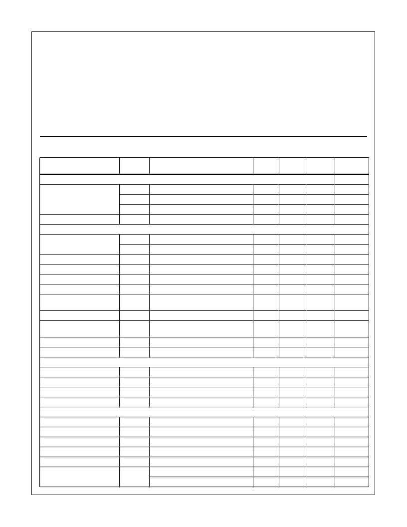
3
Absolute Maximum Ratings
T
A
= 25
o
C
Thermal Information
Supply Pins
. . . . . . . . . . . . . . . . . . . . . . . . . . . . . . . . . . . . . . . . . . . .±
5.5V
Analog Input Voltage to Ground . . . . . . . . . . . .V
DD
+0.5, V
SS
-0.5V
Digital Input Voltage to Ground. . . . . . . . . . . . . . . .V
DD
+0.5V, -0.5V
Operating Conditions
Temperature Range . . . . . . . . . . . . . . . . . . . . . . . . . . -40
o
C to 85
o
C
Thermal Resistance (Typical, Note 1)
MQFP . . . . . . . . . . . . . . . . . . . . . . . . . . . . . . . . . . .
Maximum Power Dissipation. . . . . . . . . . . . . . . . . . . . . . . . . . . . . 1.18W
Maximum Junction Temperature (T
J
) . . . . . . . . . . . . . . . . . . . . 150
o
C
Maximum Storage Temperature Range . . . . . . . . . .-65
o
C to 150
o
C
Maximum Lead Temperature (Soldering 10s). . . . . . . . . . . . . 300
o
C
(Lead Tips Only)
θ
JA
(
o
C/W)
55
CAUTION: Stresses above those listed in “Absolute Maximum Ratings” may cause permanent damage to the device. This is a stress only rating and operation
of the device at these or any other conditions above those indicated in the operational sections of this specification is not implied.
NOTE:
1.
θ
JA
is measured with the component mounted on an evaluation PC board in free air.
Electrical Specifications
V
DD
= 5V, V
SS
= -5V, R
L
Open, Over Temperature Range; Unless Otherwise Specified. Designed for
±
5%
Power Supply.
PARAMETER
SYMBOL
TEST
CONDITIONS
MIN
TYP
MAX
UNITS
OVERALL
Supply Currents
I
DD
I
SS
I
CC
PD
V
DD
(Note 2)
V
SS
(Note 3)
V
CC
Quiescent, No Load
-
66
-
mA
-
-79
-
mA
-
0
-
μ
A
Power Dissipation
-
725
-
mW
DIGITAL INTERFACE
Input Voltage Thresholds
V
IL
V
IH
I
IL
I
IH
T1
-
-
0.8
V
2.7
-
-
V
Input Currents
V
IN
= 0V
V
IN
= V
DD
-10.0
0
10.0
μ
A
-10.0
0
10.0
μ
A
Serial Clock Period
0.1
-
5.0
μ
s
CS Active Before Shift Edge
T2
T1/2 -10
-
-
ns
Write Data Valid After Shift
Edge
T3
-
-
10
ns
CS Inactive After Latch Edge
T4
T1 - 10
-
T1 +10
ns
Write Data Hold After Latch
Edge
T5
T1/2 -5
-
T1/2 +5
ns
DAC Setup Time
t
S
t
H
-
-
100
ns
DAC Hold Time
-
-
100
ns
14-BIT DAC
Resolution/Monotonicity
14
-
-
Bits
Integral Linearity
I
LE
D
LE
Measured at T
X
Outputs
-
±
1.5
-
LSB
Differential Linearity
-
±
0.9
-
LSB
Max Sample Rate
4.416
-
-
Ms/s
TRANSMITTER OUTPUT
Output Drive
TXOD
Sink or Source
30
55
-
mA
Differential Output Swing
TXOS
R
L
= 220
Gain Match Between Outputs
11.7
12.03
12.3
V
PP
%
Differential Balance
TXDB
-
0.5
-
Transmit Output Offset
TXOFF
Max Gain Single Ended (Note 4)
-200
25
200
mV
Multi-Tone Power Ratio
TXMTPR
R
L
= 220
Input Referred - V
DD
Input Referred - V
SS
-
65
-
dB
Power Supply Rejection
PSRR
40
65
-
dB
55
84
-
dB
HC6094
相關(guān)PDF資料 |
PDF描述 |
|---|---|
| HC6616JCHZC | x8 ROM (Mask Programmable) |
| HC6616JCHZT | x8 ROM (Mask Programmable) |
| HC6616JSHZC | x8 ROM (Mask Programmable) |
| HC6616JSHZT | x8 ROM (Mask Programmable) |
| HC6616KCHZC | x8 ROM (Mask Programmable) |
相關(guān)代理商/技術(shù)參數(shù) |
參數(shù)描述 |
|---|---|
| HC6094IN | 制造商:Rochester Electronics LLC 功能描述:- Bulk |
| HC-60T | 制造商:Taiyo Electric Ind. 功能描述: |
| HC6116JCHCT | 制造商:未知廠家 制造商全稱:未知廠家 功能描述:x8 SRAM |
| HC6116JCHDT | 制造商:未知廠家 制造商全稱:未知廠家 功能描述:x8 SRAM |
| HC6116JSHCT | 制造商:未知廠家 制造商全稱:未知廠家 功能描述:x8 SRAM |
發(fā)布緊急采購(gòu),3分鐘左右您將得到回復(fù)。