- 您現(xiàn)在的位置:買賣IC網(wǎng) > PDF目錄299031 > EP20K200BC784-2 (ALTERA CORP) LOADABLE PLD, PBGA784 PDF資料下載
參數(shù)資料
| 型號: | EP20K200BC784-2 |
| 廠商: | ALTERA CORP |
| 元件分類: | PLD |
| 英文描述: | LOADABLE PLD, PBGA784 |
| 文件頁數(shù): | 4/65頁 |
| 文件大?。?/td> | 781K |
| 代理商: | EP20K200BC784-2 |
第1頁第2頁第3頁當前第4頁第5頁第6頁第7頁第8頁第9頁第10頁第11頁第12頁第13頁第14頁第15頁第16頁第17頁第18頁第19頁第20頁第21頁第22頁第23頁第24頁第25頁第26頁第27頁第28頁第29頁第30頁第31頁第32頁第33頁第34頁第35頁第36頁第37頁第38頁第39頁第40頁第41頁第42頁第43頁第44頁第45頁第46頁第47頁第48頁第49頁第50頁第51頁第52頁第53頁第54頁第55頁第56頁第57頁第58頁第59頁第60頁第61頁第62頁第63頁第64頁第65頁
34
Altera Corporation
APEX 20K Programmable Logic Device Family Data Sheet
Preliminary Information
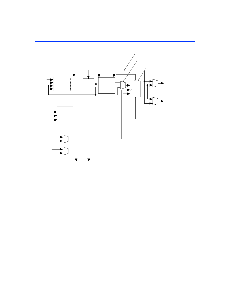
Figure 5. APEX 20K Logic Element
Each LE’s programmable register can be configured for D, T, JK, or SR
operation. The register’s clock and clear control signals can be driven by
global signals, general-purpose I/O pins, or any internal logic. For
combinatorial functions, the register is bypassed and the output of the
LUT drives the outputs of the LE.
The LE has two outputs that drive the local, MegaLAB, or FastTrack
Interconnect routing structure. Each output can be driven independently
by the LUT’s or register’s output. For example, the LUT can drive one
output while the register drives the other output. This feature, called
register packing, improves device utilization because the register and the
LUT can be used for unrelated functions. The LE can also drive out
registered and unregistered versions of the LUT output.
labclk1
labclk2
labclr1
labclr2
Carry-In
Clock &
Clock Enable
Select
Carry-Out
Look-Up
Table
(LUT)
Carry
Chain
Cascade
Chain
Cascade-In
Cascade-Out
To FastTrack Interconnect,
MegaLAB Interconnect,
or Local Interconnect
To FastTrack Interconnect,
MegaLAB Interconnect,
or Local Interconnect
Programmable
Register
PRN
CLRN
D
Q
ENA
Register Bypass
Packed
Register Select
Chip-Wide
Reset
labclkena1
labclkena2
Synchronous
Load & Clear
Logic
LAB-wide
Synchronous
Load
LAB-wide
Synchronous
Clear
Asynchronous
Clear/Preset/
Load Logic
data1
data2
data3
data4
相關(guān)PDF資料 |
PDF描述 |
|---|---|
| EP20K200BC784-3 | LOADABLE PLD, PBGA784 |
| EP20K200BI784-1 | LOADABLE PLD, PBGA784 |
| EP20K200BI784-2 | LOADABLE PLD, PBGA784 |
| EP20K200BI784-3 | LOADABLE PLD, PBGA784 |
| EP20K200EFC784-1 | LOADABLE PLD, PBGA784 |
相關(guān)代理商/技術(shù)參數(shù) |
參數(shù)描述 |
|---|---|
| EP20K200BI356-1ES | 制造商:未知廠家 制造商全稱:未知廠家 功能描述:FPGA |
| EP20K200BI356-2ES | 制造商:未知廠家 制造商全稱:未知廠家 功能描述:FPGA |
| EP20K200BI356-3ES | 制造商:未知廠家 制造商全稱:未知廠家 功能描述:FPGA |
| EP20K200C | 制造商:ALTERA 制造商全稱:Altera Corporation 功能描述:Programmable Logic |
| EP20K200CB356C7 | 制造商:Altera Corporation 功能描述:IC APEX 20KC FPGA 356BGA |
發(fā)布緊急采購,3分鐘左右您將得到回復。