- 您現(xiàn)在的位置:買賣IC網(wǎng) > PDF目錄378516 > CYP15G0401DXB-BGI (CYPRESS SEMICONDUCTOR CORP) Quad HOTLink II Transceiver PDF資料下載
參數(shù)資料
| 型號(hào): | CYP15G0401DXB-BGI |
| 廠商: | CYPRESS SEMICONDUCTOR CORP |
| 元件分類: | 通信及網(wǎng)絡(luò) |
| 英文描述: | Quad HOTLink II Transceiver |
| 中文描述: | SPECIALTY TELECOM CIRCUIT, PBGA256 |
| 封裝: | BGA-256 |
| 文件頁(yè)數(shù): | 27/48頁(yè) |
| 文件大?。?/td> | 1115K |
| 代理商: | CYP15G0401DXB-BGI |
第1頁(yè)第2頁(yè)第3頁(yè)第4頁(yè)第5頁(yè)第6頁(yè)第7頁(yè)第8頁(yè)第9頁(yè)第10頁(yè)第11頁(yè)第12頁(yè)第13頁(yè)第14頁(yè)第15頁(yè)第16頁(yè)第17頁(yè)第18頁(yè)第19頁(yè)第20頁(yè)第21頁(yè)第22頁(yè)第23頁(yè)第24頁(yè)第25頁(yè)第26頁(yè)當(dāng)前第27頁(yè)第28頁(yè)第29頁(yè)第30頁(yè)第31頁(yè)第32頁(yè)第33頁(yè)第34頁(yè)第35頁(yè)第36頁(yè)第37頁(yè)第38頁(yè)第39頁(yè)第40頁(yè)第41頁(yè)第42頁(yè)第43頁(yè)第44頁(yè)第45頁(yè)第46頁(yè)第47頁(yè)第48頁(yè)
CYP15G0401DXA
PRELIMINARY
Document #: 38-02002 Rev. *B
Page 27 of 48
range of system environments, the CYP15G0401DXA sup-
ports multiple different forms of parity generation (in addition
to no parity). When the decoders are enabled (DECMODE
≠
LOW), parity can be generated on
the RXDx[7:0] character
the RXDx[7:0] character and RXSTx[2:0] status
When the decoders are bypassed (DECMODE = LOW), parity
can be generated on
the RXDx[7:0] and RXSTx[1:0] bits
the RXDx[7:0] and RXSTx[2:0] bits
These modes differ in the number bits which are included in
the parity calculation. For all cases, only ODD parity is provid-
ed which ensures that at least one bit of the data bus is always
a logic-1. Those bits covered by parity generation are listed in
Table 20
.
Parity generation is enabled through the 3-level select
PARCTL input. When PARCTL = LOW, parity checking is dis-
abled, and the RXOPx outputs are all disabled (High-Z).
When PARCTL is MID (open) and the decoders are enabled
(DECMODE
≠
LOW), ODD parity is generated for the received
and decoded character in the RXDx[7:0] signals and is pre-
sented on the associated RXOPx output. When PARCTL is
MID (open) and the decoders are bypassed
(DECMODE
=
LOW), ODD parity is generated for the received
and decoded character in the RXDx[7:0] and RXSTx[1:0] bit
positions.
When PARCTL = HIGH with the decoder enabled (or by-
passed), ODD parity is generated for both the received and
decoded character, and for the associated RXSTx[2:0] status
bits.
When interface clocking is such that the decoded character is
passed through the receive Elasticity Buffer prior to the addi-
tion of the RXSTx[2:0] status bits, the generation of output
parity becomes a two-step process. The first parity calculation
takes place as soon as the character is framed and decoded.
This generates proper parity for the data portion of the decod-
ed character which is then written to the Elasticity Buffer. When
the parity calculation also includes the associated RXSTx[2:0]
status bits (PARCTL = HIGH), a second parity calculation is
made prior to loading the data and status bits into the receive
Output Register. This is necessary because the status bits as-
sociated with a character in the Output Register are not nec-
essarily determined until after the character is read from the
receive Elasticity Buffer.
This second parity calculation is based only on the content of
the status bits, and the singular parity bit associated with the
character read from the Elasticity Buffer.
Receive Status Bits
When the 10B/8B decoder is enabled (DECMODE
≠
LOW),
each character presented at the output register includes three
associated status bits. These bits are used to identify
if the contents of the data bus are valid,
the type of character present,
the state of receive BIST operations (regardless of the state
of DECMODE),
character violations,
and channel bonding status.
These conditions normally overlap; i.e., a valid data character
received with incorrect running disparity is not reported as a
valid data character. It is instead reported as a decoder viola-
tion of some specific type. This implies a hierarchy or priority
level to the various status bit combinations. The hierarchy and
value of each status is listed in
Table 21
.
Within these status decodes, there are three forms of status
reporting. The two normal or data status reporting modes
(Type A and Type B) are selectable through the RXMODE[0]
input. These status types allow compatibility with legacy sys-
tems, while allowing full reporting in new systems. The third
status type is used for reporting receive BIST status and
progress. These status values are generated in part by the
Receive Synchronization State Machine, and are listed in
Table 21
.
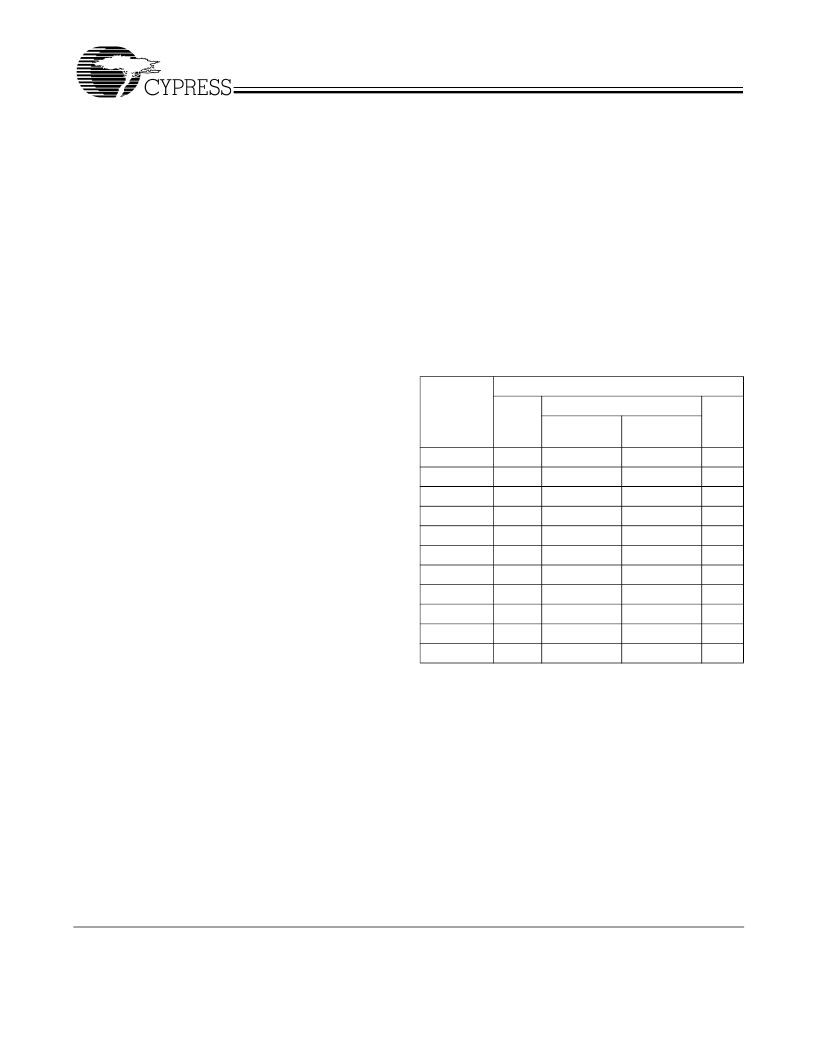
Notes:
9.
10. Receive path parity output drivers (RXOPx) are disabled (High-Z) when PARCTL = LOW
when the character in the output buffer is a framing character.
Table 20. Output Register Parity Generation
Signal
Name
RXSTx[2]
RXSTx[1]
RXSTx[0]
RXDx[0]
RXDx[1]
RXDx[2]
RXDx[3]
RXDx[4]
RXDx[5]
RXDx[6]
RXDx[7]
Receive Parity Generate Mode (PARCTL)
MID
DECMODE
= LOW
LOW
[9]
HIGH
X
[10]
X
X
X
X
X
X
X
X
X
X
DECMODE
≠
LOW
X
X
X
X
X
X
X
X
X
X
X
X
X
X
X
X
X
X
相關(guān)PDF資料 |
PDF描述 |
|---|---|
| CYP15G0401DXA-BGC | Quad HOTLink II Transceiver |
| CYP15G0401DXA-BGI | Quad HOTLink II Transceiver |
| CYRF6936 | WirelessUSB LP 2.4GHz Radio SoC(WirelessUSB LP 2.4GHz無(wú)線SoC) |
| CYV15G0104TRB | Independent Clock HOTLink II Serializer and Reclocking Deserializer(獨(dú)立時(shí)鐘,HOTLink II并串轉(zhuǎn)換器及時(shí)鐘恢復(fù)串并轉(zhuǎn)換器) |
| CYV15G0201DXB-BBI | Dual-channel HOTLink II Transceiver |
相關(guān)代理商/技術(shù)參數(shù) |
參數(shù)描述 |
|---|---|
| CYP15G0401DXB-BGXC | 功能描述:電信線路管理 IC Dual Channel XCVR 1.5Gbps Bckplane COM RoHS:否 制造商:STMicroelectronics 產(chǎn)品:PHY 接口類型:UART 電源電壓-最大:18 V 電源電壓-最小:8 V 電源電流:30 mA 最大工作溫度:+ 85 C 最小工作溫度:- 40 C 安裝風(fēng)格:SMD/SMT 封裝 / 箱體:VFQFPN-48 封裝:Tray |
| CYP15G0401DXB-BGXCKG | 制造商:Rochester Electronics LLC 功能描述: 制造商:Cypress Semiconductor 功能描述: |
| CYP15G0401DXBBGXI | 制造商:Cypress Semiconductor 功能描述: |
| CYP15G0401DXB-BGXI | 功能描述:電信線路管理 IC Quad HOTLink II XCVR Ch 1.5Gbps Backplane RoHS:否 制造商:STMicroelectronics 產(chǎn)品:PHY 接口類型:UART 電源電壓-最大:18 V 電源電壓-最小:8 V 電源電流:30 mA 最大工作溫度:+ 85 C 最小工作溫度:- 40 C 安裝風(fēng)格:SMD/SMT 封裝 / 箱體:VFQFPN-48 封裝:Tray |
| CYP15G0401DX-BGC | 制造商:Rochester Electronics LLC 功能描述:- Bulk |
發(fā)布緊急采購(gòu),3分鐘左右您將得到回復(fù)。