- 您現(xiàn)在的位置:買賣IC網(wǎng) > PDF目錄379098 > CYD36S36V18 (Cypress Semiconductor Corp.) FullFlex Synchronous SDR Dual-Port SRAM(FullFlex同步SDR雙端口SRAM) PDF資料下載
參數(shù)資料
| 型號(hào): | CYD36S36V18 |
| 廠商: | Cypress Semiconductor Corp. |
| 英文描述: | FullFlex Synchronous SDR Dual-Port SRAM(FullFlex同步SDR雙端口SRAM) |
| 中文描述: | FullFlex器件特別提款權(quán)同步雙端口SRAM(FullFlex器件同步雙端口SRAM的特別提款權(quán)) |
| 文件頁數(shù): | 8/52頁 |
| 文件大小: | 774K |
| 代理商: | CYD36S36V18 |
第1頁第2頁第3頁第4頁第5頁第6頁第7頁當(dāng)前第8頁第9頁第10頁第11頁第12頁第13頁第14頁第15頁第16頁第17頁第18頁第19頁第20頁第21頁第22頁第23頁第24頁第25頁第26頁第27頁第28頁第29頁第30頁第31頁第32頁第33頁第34頁第35頁第36頁第37頁第38頁第39頁第40頁第41頁第42頁第43頁第44頁第45頁第46頁第47頁第48頁第49頁第50頁第51頁第52頁
FullFlex
Document #: 38-06082 Rev. *F
Page 8 of 52
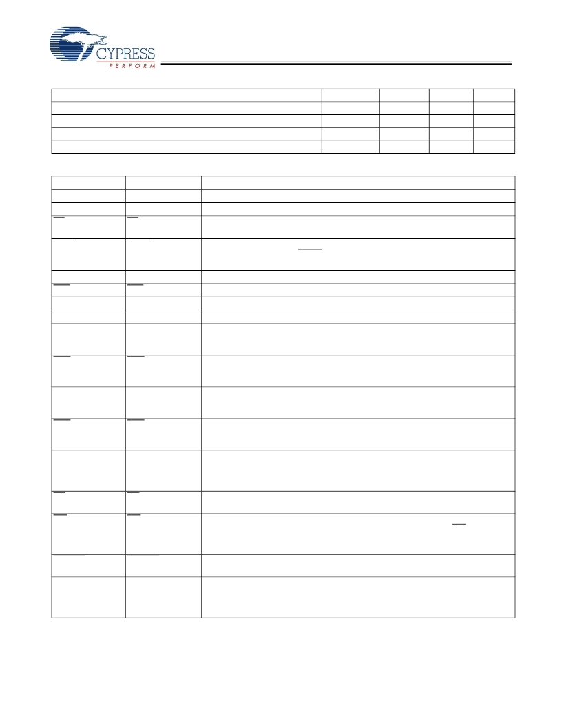
Table 1. Selection Guide
–250
250
2.64
930
[14]
210
[14]
–200
200
3.3
800
[14]
210
[14]
–167
167
4.0
700
[14]
210
[14]
Unit
MHz
ns
mA
mA
f
MAX[15]
Max. Access Time (Clock to Data)
Typical Operating Current I
CC
Typical Standby Current for I
SB3
(Both Ports CMOS Level)
Pin Definitions
Left Port
Right Port
A[20:0]
R
DQ[71:0]
R
BE[7:0]
R
Description
A[20:0]
L
DQ[71:0]
L
BE[7:0]
L
Address Inputs
.
[1]
Data Bus Input/Output
.
[2]
Byte Select Inputs
.
[3]
Asserting these signals enables Read and Write operations to
the corresponding bytes of the memory array.
Port Busy Output
. When there is an address match and both chip enables are active
for both ports, an external BUSY signal is asserted on the fifth clock cycles from when
the collision occurs.
Clock Signal
. Maximum clock input rate is f
MAX
.
Active LOW Chip Enable Input
.
Active HIGH Chip Enable Input
.
Echo Clock Enable Input
. Assert HIGH to enable echo clocking on respective port.
Echo Clock Signal Output for DQ[35:0] for FullFlex72 devices
. Echo Clock Signal
Output for DQ[17:0] for FullFlex36 devices. Echo Clock Signal Output for DQ[8:0] for
FullFlex18 devices.
Inverted Echo Clock Signal Output for DQ[35:0] for FullFlex72 devices
. Inverted
Echo Clock Signal Output for DQ[17:0] for FullFlex36 devices. Inverted Echo Clock
Signal Output for DQ[8:0] for FullFlex18 devices.
Echo Clock Signal Output for DQ[71:36] for FullFlex72 devices
. Echo Clock Signal
Output for DQ[35:18] for FullFlex36 devices. Echo Clock Signal Output for DQ[17:9]
for FullFlex18 devices.
Inverted Echo Clock Signal Output for DQ[71:36] for FullFlex72 devices
. Inverted
Echo Clock Signal Output for DQ[35:18] for FullFlex36 devices. Inverted Echo Clock
Signal Output for DQ[17:9] forFullFlex18 devices.
VIM Output Impedance Matching Input
. To use, connect a calibrating resistor
between ZQ and ground. The resistor must be five times larger than the intended line
impedance driven by the dual-port. Assert HIGH or leave NC to disable Variable
Impedance Matching.
Output Enable Input
. This asynchronous signal must be asserted LOW to enable the
DQ data pins during Read operations.
Mailbox Interrupt Flag Output
.
The mailbox permits communications between ports.
The upper two memory locations can be used for message passing. INT
L
is asserted
LOW when the right port writes to the mailbox location of the left port, and vice versa.
An interrupt to a port is deasserted HIGH when it reads the contents of its mailbox.
Port Low Speed Select Input
.
Assert this pin LOW to disable the DLL. For operation
at less than 100 MHz, assert this pin LOW.
PORTSTD[1:0]
L[16]
PORTSTD[1:0]
R[16]
Port Clock/Address/Control/Data/Echo Clock/I/O Standard Select Input
. Assert
these pins LOW/LOW for LVTTL, LOW/HIGH for HSTL, HIGH/LOW for 2.5V LVCMOS,
and HIGH/HIGH for 1.8V LVCMOS, respectively. These pins must be driven by VTTL
referenced levels.
BUSY
L
BUSY
R
C
L
CE0
L
CE1
L
CQEN
L
CQ0
L
C
R
CE0
R
CE1
R
CQEN
R
CQ0
R
CQ0
L
CQ0
R
CQ1
L
CQ1
R
CQ1
L
CQ1
R
ZQ[1:0]
L
ZQ[1:0]
R
OE
L
OE
R
INT
L
INT
R
LowSPD
L
LowSPD
R
Notes:
14.For 18-Mbit x72 commercial configuration only, please refer to the electrical characteristics section for complete information.
15.SDR mode with two pipelined stages.
16.PORTSTD[1:0]
L
and PORTSTD[1:0]
R
have internal pull-down resistors.
相關(guān)PDF資料 |
PDF描述 |
|---|---|
| CYD18S72V | FLEx72 3.3V 64K/128K/256K x 72 Synchronous Dual-Port RAM(FLEx72 3.3V 64K/128K/256K x 72同步雙端口RAM) |
| CYD09S72V | FLEx72 3.3V 64K/128K/256K x 72 Synchronous Dual-Port RAM(FLEx72 3.3V 64K/128K/256K x 72同步雙端口RAM) |
| CYDC128B08-55AXC | 1.8V 4k/8k/16k x 16 and 8k/16k x 8 ConsuMoBL Dual-Port Static RAM |
| CYDC064B08 | 1.8V 4k/8k/16k x 16 and 8k/16k x 8 ConsuMoBL Dual-Port Static RAM |
| CYDC064B08-40AXC | 1.8V 4k/8k/16k x 16 and 8k/16k x 8 ConsuMoBL Dual-Port Static RAM |
相關(guān)代理商/技術(shù)參數(shù) |
參數(shù)描述 |
|---|---|
| CYD36S36V18-133BBXC | 功能描述:IC SRAM 36MBIT 133MHZ 256LFBGA RoHS:是 類別:集成電路 (IC) >> 存儲(chǔ)器 系列:- 標(biāo)準(zhǔn)包裝:1,000 系列:- 格式 - 存儲(chǔ)器:RAM 存儲(chǔ)器類型:移動(dòng) SDRAM 存儲(chǔ)容量:256M(8Mx32) 速度:133MHz 接口:并聯(lián) 電源電壓:1.7 V ~ 1.95 V 工作溫度:-40°C ~ 85°C 封裝/外殼:90-VFBGA 供應(yīng)商設(shè)備封裝:90-VFBGA(8x13) 包裝:帶卷 (TR) 其它名稱:557-1327-2 |
| CYD36S36V18-133BBXI | 功能描述:IC SRAM 36MBIT 133MHZ 256LFBGA RoHS:是 類別:集成電路 (IC) >> 存儲(chǔ)器 系列:- 標(biāo)準(zhǔn)包裝:1,000 系列:- 格式 - 存儲(chǔ)器:RAM 存儲(chǔ)器類型:移動(dòng) SDRAM 存儲(chǔ)容量:256M(8Mx32) 速度:133MHz 接口:并聯(lián) 電源電壓:1.7 V ~ 1.95 V 工作溫度:-40°C ~ 85°C 封裝/外殼:90-VFBGA 供應(yīng)商設(shè)備封裝:90-VFBGA(8x13) 包裝:帶卷 (TR) 其它名稱:557-1327-2 |
| CYD36S36V18-167BBC | 制造商:Cypress Semiconductor 功能描述:SRAM SYNC DUAL 1.8V 36MBIT 1MX36 11NS/6NS 484BGA - Bulk |
| CYD36S36V18-167BBXC | 功能描述:IC SRAM 36MBIT 167MHZ 256LFBGA RoHS:是 類別:集成電路 (IC) >> 存儲(chǔ)器 系列:- 標(biāo)準(zhǔn)包裝:1,000 系列:- 格式 - 存儲(chǔ)器:RAM 存儲(chǔ)器類型:移動(dòng) SDRAM 存儲(chǔ)容量:256M(8Mx32) 速度:133MHz 接口:并聯(lián) 電源電壓:1.7 V ~ 1.95 V 工作溫度:-40°C ~ 85°C 封裝/外殼:90-VFBGA 供應(yīng)商設(shè)備封裝:90-VFBGA(8x13) 包裝:帶卷 (TR) 其它名稱:557-1327-2 |
| CYD36S36V18-167BBXI | 功能描述:IC SRAM 36MBIT 167MHZ 256LFBGA RoHS:是 類別:集成電路 (IC) >> 存儲(chǔ)器 系列:- 標(biāo)準(zhǔn)包裝:1,000 系列:- 格式 - 存儲(chǔ)器:RAM 存儲(chǔ)器類型:移動(dòng) SDRAM 存儲(chǔ)容量:256M(8Mx32) 速度:133MHz 接口:并聯(lián) 電源電壓:1.7 V ~ 1.95 V 工作溫度:-40°C ~ 85°C 封裝/外殼:90-VFBGA 供應(yīng)商設(shè)備封裝:90-VFBGA(8x13) 包裝:帶卷 (TR) 其它名稱:557-1327-2 |
發(fā)布緊急采購,3分鐘左右您將得到回復(fù)。