- 您現(xiàn)在的位置:買賣IC網(wǎng) > PDF目錄379098 > CYD04S72V18 (Cypress Semiconductor Corp.) FullFlex Synchronous SDR Dual-Port SRAM(FullFlex同步SDR雙端口SRAM) PDF資料下載
參數(shù)資料
| 型號: | CYD04S72V18 |
| 廠商: | Cypress Semiconductor Corp. |
| 英文描述: | FullFlex Synchronous SDR Dual-Port SRAM(FullFlex同步SDR雙端口SRAM) |
| 中文描述: | FullFlex器件特別提款權(quán)同步雙端口SRAM(FullFlex器件同步雙端口SRAM的特別提款權(quán)) |
| 文件頁數(shù): | 9/52頁 |
| 文件大小: | 774K |
| 代理商: | CYD04S72V18 |
第1頁第2頁第3頁第4頁第5頁第6頁第7頁第8頁當(dāng)前第9頁第10頁第11頁第12頁第13頁第14頁第15頁第16頁第17頁第18頁第19頁第20頁第21頁第22頁第23頁第24頁第25頁第26頁第27頁第28頁第29頁第30頁第31頁第32頁第33頁第34頁第35頁第36頁第37頁第38頁第39頁第40頁第41頁第42頁第43頁第44頁第45頁第46頁第47頁第48頁第49頁第50頁第51頁第52頁
FullFlex
Document #: 38-06082 Rev. *F
Page 9 of 52
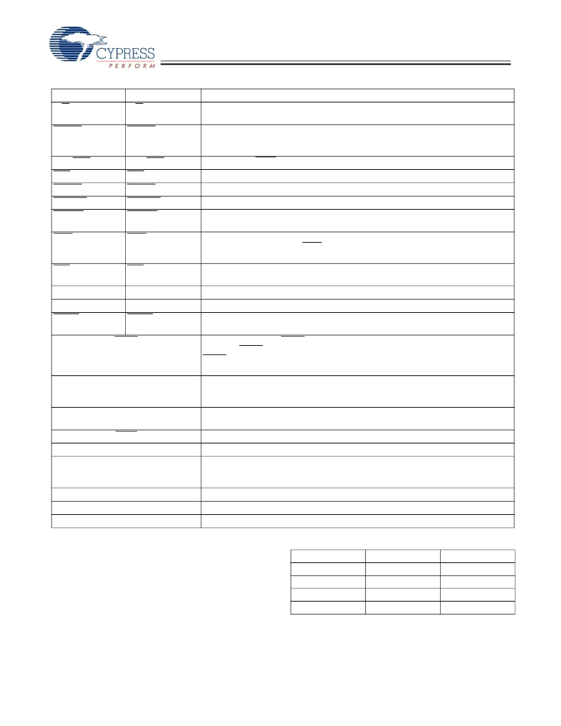
Selectable I/O Standard
The FullFlex device families also offer the option of choosing
one of four port standards for the device. Each port can
independently select standards from single-ended HSTL class
I, single-ended LVTTL, 2.5V LVCMOS, or 1.8V LVCMOS. The
selection of the standard is determined by the PORTSTD pins
for each port. These pins should be connected to either an
LVTTL or 2.5V LVCMOS power suppy. This will determine the
input clock, address, control, data, and Echo clock standard
for each port as shown in
Table 2
. Please note that only 1.8V
LVCMOS and HSTL are supported for 4-Mbit, 9-Mbit, 18-Mbit
devices running at 250 MHz, and for 36-Mbit devices running
at 200 MHz.
Table 2. Port Standard Selection
Clocking
Separate clocks synchronize the operations on each port.
Each port has one clock input C. In this mode, all the transac-
tions on the address, control, and data will be on the C rising
R/W
L
R/W
R
Read/Write Enable Input
. Assert this pin LOW to Write to, or HIGH to Read from the
dual-port memory array.
Port DLL Ready Output
. This signal will be asserted LOW when the DLL and Variable
Impedance Matching circuits have completed calibration. This is a wired OR capable
output.
Port Counter/Mask Select Input
.
Counter control input.
Port Counter Address Load Strobe Input
.
Counter control input.
Port Counter Enable Input
.
Counter control input.
Port Counter Reset Input
. Counter control input.
Port Counter Interrupt Output
. This pin is asserted LOW one cycle before the
unmasked portion of the counter is incremented to all “1s”.
Port Counter Wrap Input
.
When the burst counter reaches the maximum count, on
the next counter increment WRP can be set LOW to load the unmasked counter bits
to 0 or set HIGH to load the counter with the value stored in the mirror register.
Port Counter Retransmit Input
.
Assert this pin LOW to reload the initial address for
repeated access to the same segment of memory.
Port External HSTL I/O Reference Input
. This pin is left NC when HSTL is not used.
Port Data I/O Power Supply
.
Port Flow-through Mode Select Input
.
Assert this pin LOW to select Flow-through
mode. Assert this pin HIGH to select Pipelined mode.
Master Reset Input
. MRST is an asynchronous input signal and affects both ports.
Asserting MRST LOW performs all of the reset functions as described in the text. A
MRST operation is required at power-up. This pin must be driven by a VDDIO
L
refer-
enced signal.
JTAG Test Mode Select Input
. It controls the advance of JTAG TAP state machine.
State machine transitions occur on the rising edge of TCK. Operation for LVTTL or 2.5V
LVCMOS.
JTAG Test Data Input
. Data on the TDI input will be shifted serially into selected
registers. Operation for LVTTL or 2.5V LVCMOS.
JTAG Reset Input
. Operation for LVTTL or 2.5V LVCMOS.
JTAG Test Clock Input
. Operation for LVTTL or 2.5V LVCMOS.
JTAG Test Data Output
. TDO transitions occur on the falling edge of TCK. TDO is
normally three-stated except when captured data is shifted out of the JTAG TAP.
Operation for LVTTL or 2.5V LVCMOS.
Ground Inputs
.
Device Core Power Supply
.
LVTTL Power Supply
.
READY
L
READY
R
CNT/MSK
L
ADS
L
CNTEN
L
CNTRST
L
CNTINT
L
CNT/MSK
R
ADS
R
CNTEN
R
CNTRST
R
CNTINT
R
WRP
L
WRP
R
RET
L
RET
R
VREF
L
VDDIO
L
FTSEL
L
VREF
R
VDDIO
R
FTSEL
R
MRST
TMS
TDI
TRST
TCK
TDO
VSS
VCORE
VTTL
Pin Definitions
(continued)
Left Port
Right Port
Description
PORTSTD1
VSS
VSS
VTTL
VTTL
PORTSTD0
VSS
VTTL
VSS
VTTL
I/O Standard
LVTTL
HSTL
2.5V LVCMOS
1.8V LVCMOS
相關(guān)PDF資料 |
PDF描述 |
|---|---|
| CYD36S72V18 | FullFlex Synchronous SDR Dual-Port SRAM(FullFlex同步SDR雙端口SRAM) |
| CYD09S72V18 | FullFlex Synchronous SDR Dual-Port SRAM(FullFlex同步SDR雙端口SRAM) |
| CYD36S18V18 | FullFlex Synchronous SDR Dual-Port SRAM(FullFlex同步SDR雙端口SRAM) |
| CYD36S36V18 | FullFlex Synchronous SDR Dual-Port SRAM(FullFlex同步SDR雙端口SRAM) |
| CYD18S72V | FLEx72 3.3V 64K/128K/256K x 72 Synchronous Dual-Port RAM(FLEx72 3.3V 64K/128K/256K x 72同步雙端口RAM) |
相關(guān)代理商/技術(shù)參數(shù) |
參數(shù)描述 |
|---|---|
| CYD04S72V18-167BBXC | 功能描述:靜態(tài)隨機(jī)存取存儲器 4M Sync Dual Port 64Kx72 90nm COM RoHS:否 制造商:Cypress Semiconductor 存儲容量:16 Mbit 組織:1 M x 16 訪問時間:55 ns 電源電壓-最大:3.6 V 電源電壓-最小:2.2 V 最大工作電流:22 uA 最大工作溫度:+ 85 C 最小工作溫度:- 40 C 安裝風(fēng)格:SMD/SMT 封裝 / 箱體:TSOP-48 封裝:Tray |
| CYD04S72V18-167BBXI | 功能描述:靜態(tài)隨機(jī)存取存儲器 4M Sync Dual Port 64Kx72 90nm IND RoHS:否 制造商:Cypress Semiconductor 存儲容量:16 Mbit 組織:1 M x 16 訪問時間:55 ns 電源電壓-最大:3.6 V 電源電壓-最小:2.2 V 最大工作電流:22 uA 最大工作溫度:+ 85 C 最小工作溫度:- 40 C 安裝風(fēng)格:SMD/SMT 封裝 / 箱體:TSOP-48 封裝:Tray |
| CYD04S72V18-200BBXC | 功能描述:靜態(tài)隨機(jī)存取存儲器 4M Sync Dual Port 64Kx72 90nm COM RoHS:否 制造商:Cypress Semiconductor 存儲容量:16 Mbit 組織:1 M x 16 訪問時間:55 ns 電源電壓-最大:3.6 V 電源電壓-最小:2.2 V 最大工作電流:22 uA 最大工作溫度:+ 85 C 最小工作溫度:- 40 C 安裝風(fēng)格:SMD/SMT 封裝 / 箱體:TSOP-48 封裝:Tray |
| CYD04S72V18-200BBXI | 功能描述:靜態(tài)隨機(jī)存取存儲器 4M Sync Dual Port 64Kx72 90nm IND RoHS:否 制造商:Cypress Semiconductor 存儲容量:16 Mbit 組織:1 M x 16 訪問時間:55 ns 電源電壓-最大:3.6 V 電源電壓-最小:2.2 V 最大工作電流:22 uA 最大工作溫度:+ 85 C 最小工作溫度:- 40 C 安裝風(fēng)格:SMD/SMT 封裝 / 箱體:TSOP-48 封裝:Tray |
| CYD04S72V18-250BBXC | 功能描述:靜態(tài)隨機(jī)存取存儲器 4M Sync Dual Port 64Kx72 90nm COM RoHS:否 制造商:Cypress Semiconductor 存儲容量:16 Mbit 組織:1 M x 16 訪問時間:55 ns 電源電壓-最大:3.6 V 電源電壓-最小:2.2 V 最大工作電流:22 uA 最大工作溫度:+ 85 C 最小工作溫度:- 40 C 安裝風(fēng)格:SMD/SMT 封裝 / 箱體:TSOP-48 封裝:Tray |
發(fā)布緊急采購,3分鐘左右您將得到回復(fù)。