- 您現(xiàn)在的位置:買賣IC網(wǎng) > PDF目錄378513 > CY8C21323 (Cypress Semiconductor Corp.) PSoC Mixed-Signal Array(PSoC混合信號陣列) PDF資料下載
參數(shù)資料
| 型號: | CY8C21323 |
| 廠商: | Cypress Semiconductor Corp. |
| 英文描述: | PSoC Mixed-Signal Array(PSoC混合信號陣列) |
| 中文描述: | PSoC混合信號陣列(的PSoC混合信號陣列) |
| 文件頁數(shù): | 16/33頁 |
| 文件大小: | 325K |
| 代理商: | CY8C21323 |
第1頁第2頁第3頁第4頁第5頁第6頁第7頁第8頁第9頁第10頁第11頁第12頁第13頁第14頁第15頁當前第16頁第17頁第18頁第19頁第20頁第21頁第22頁第23頁第24頁第25頁第26頁第27頁第28頁第29頁第30頁第31頁第32頁第33頁
February 25, 2005
Document No. 38-12022 Rev. *G
16
CY8C21x23 Final Data Sheet
3. Electrical Specifications
3.3.2
DC General Purpose IO Specifications
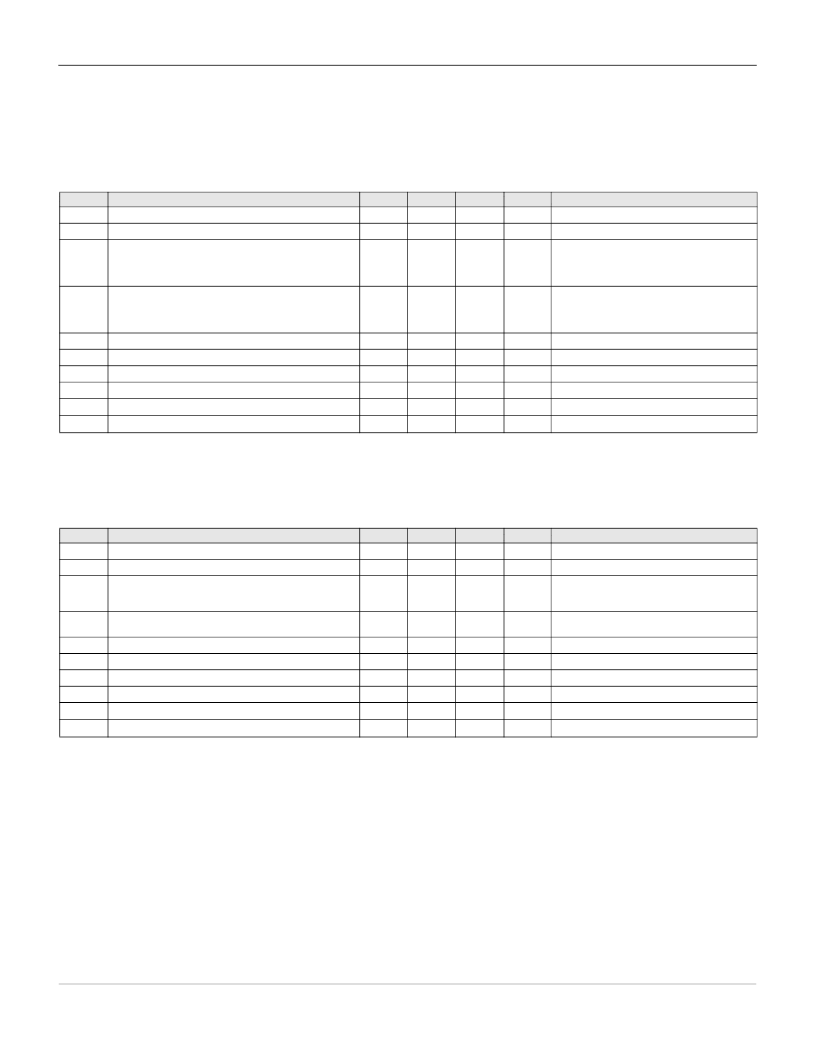
The following table lists guaranteed maximum and minimum specifications for the voltage and temperature ranges: 4.75V to 5.25V
and -40
°
C
≤
T
A
≤
85
°
C, 3.0V to 3.6V and -40
°
C
≤
T
A
≤
85
°
C, respectively. Typical parameters apply to 5V, 3.3V, or 2.7V at 25
°
C and
are for design guidance only.
The following table lists guaranteed maximum and minimum specifications for the voltage and temperature ranges: 2.4V to 3.0V and
-40
°
C
≤
T
A
≤
85
°
C. Typical parameters apply to 2.7V at 25
°
C and are for design guidance only.
Table 3-5. 5V and 3.3V DC GPIO Specifications
Symbol
R
PU
R
PD
V
OH
Description
Min
Typ
Max
Units
k
k
Notes
Pull up Resistor
4
5.6
8
Pull down Resistor
4
5.6
8
High Output Level
Vdd - 1.0
–
–
V
IOH = 10 mA, Vdd = 4.75 to 5.25V (8 total loads,
4 on even port pins (for example, P0[2], P1[4]),
4 on odd port pins (for example, P0[3], P1[5])).
80 mA maximum combined IOH budget.
IOL = 25 mA, Vdd = 4.75 to 5.25V (8 total loads,
4 on even port pins (for example, P0[2], P1[4]),
4 on odd port pins (for example, P0[3], P1[5])).
150 mA maximum combined IOL budget.
Vdd = 3.0 to 5.25.
V
OL
Low Output Level
–
–
0.75
V
V
IL
V
IH
V
H
I
IL
C
IN
C
OUT
Input Low Level
–
–
0.8
V
Input High Level
2.1
–
V
Vdd = 3.0 to 5.25.
Input Hysteresis
–
60
–
mV
Input Leakage (Absolute Value)
–
1
–
nA
Gross tested to 1
μ
A.
Capacitive Load on Pins as Input
–
3.5
10
pF
Package and pin dependent. Temp = 25
o
C.
Package and pin dependent. Temp = 25
o
C.
Capacitive Load on Pins as Output
–
3.5
10
pF
Table 3-6. 2.7V DC GPIO Specifications
Symbol
R
PU
R
PD
V
OH
Description
Min
Typ
Max
Units
k
k
Notes
Pull up Resistor
4
5.6
8
Pull down Resistor
4
5.6
8
High Output Level
Vdd - 0.4
–
–
V
IOH = 2.5 mA (6.25 Typ), Vdd = 2.4 to 3.0V (16
mA maximum, 50 mA Typ combined IOH bud-
get).
IOL = 10 mA, Vdd = 2.4 to 3.0V (90 mA maxi-
mum combined IOL budget).
Vdd = 2.4 to 3.0.
V
OL
Low Output Level
–
–
0.75
V
V
IL
V
IH
V
H
I
IL
C
IN
C
OUT
Input Low Level
–
–
0.75
V
Input High Level
2.0
–
–
V
Vdd = 2.4 to 3.0.
Input Hysteresis
–
60
–
mV
Input Leakage (Absolute Value)
–
1
–
nA
Gross tested to 1
μ
A.
Capacitive Load on Pins as Input
–
3.5
10
pF
Package and pin dependent. Temp = 25
o
C.
Package and pin dependent. Temp = 25
o
C.
Capacitive Load on Pins as Output
–
3.5
10
pF
相關(guān)PDF資料 |
PDF描述 |
|---|---|
| CY8C21123 | PSoC Mixed-Signal Array(PSoC混合信號陣列) |
| CY8C21223 | PSoC Mixed-Signal Array(PSoC混合信號陣列) |
| CY8C21634-24AX | PSoC Mixed-Signal Array |
| CY8C21534 | PSoC Mixed-Signal Array |
| CY8C21234-24LFX | PQ I HIP6W DUET |
相關(guān)代理商/技術(shù)參數(shù) |
參數(shù)描述 |
|---|---|
| CY8C21323_06 | 制造商:CYPRESS 制造商全稱:Cypress Semiconductor 功能描述:PSoC㈢ Mixed-Signal Array |
| CY8C21323_08 | 制造商:CYPRESS 制造商全稱:Cypress Semiconductor 功能描述:PSoC? Mixed Signal Array |
| CY8C21323-12PVXE | 制造商:CYPRESS 制造商全稱:Cypress Semiconductor 功能描述:PSoC㈢ Mixed-Signal Array |
| CY8C21323-12PVXET | 制造商:CYPRESS 制造商全稱:Cypress Semiconductor 功能描述:PSoC㈢ Mixed-Signal Array |
| CY8C21323-24LFXI | 功能描述:可編程片上系統(tǒng) - PSoC IC MCU 4K FLASH 256B SRAM RoHS:否 制造商:Cypress Semiconductor 核心:8051 處理器系列:CY8C36 數(shù)據(jù)總線寬度:8 bit 最大時鐘頻率:67 MHz 程序存儲器大小:32 KB 數(shù)據(jù) RAM 大小:4 KB 片上 ADC:Yes 工作電源電壓:0.5 V to 5.5 V 工作溫度范圍:- 40 C to + 85 C 封裝 / 箱體:QFN-68 安裝風格:SMD/SMT |
發(fā)布緊急采購,3分鐘左右您將得到回復。