- 您現(xiàn)在的位置:買賣IC網(wǎng) > PDF目錄378513 > CY7C63231-PC (CYPRESS SEMICONDUCTOR CORP) enCoRe USB Low-speed USB Peripheral Controller PDF資料下載
參數(shù)資料
| 型號(hào): | CY7C63231-PC |
| 廠商: | CYPRESS SEMICONDUCTOR CORP |
| 元件分類: | 微控制器/微處理器 |
| 英文描述: | enCoRe USB Low-speed USB Peripheral Controller |
| 中文描述: | 8-BIT, OTPROM, RISC MICROCONTROLLER, PDIP18 |
| 封裝: | 0.300 INCH, PLASTIC, DIP-18 |
| 文件頁(yè)數(shù): | 14/49頁(yè) |
| 文件大小: | 960K |
| 代理商: | CY7C63231-PC |
第1頁(yè)第2頁(yè)第3頁(yè)第4頁(yè)第5頁(yè)第6頁(yè)第7頁(yè)第8頁(yè)第9頁(yè)第10頁(yè)第11頁(yè)第12頁(yè)第13頁(yè)當(dāng)前第14頁(yè)第15頁(yè)第16頁(yè)第17頁(yè)第18頁(yè)第19頁(yè)第20頁(yè)第21頁(yè)第22頁(yè)第23頁(yè)第24頁(yè)第25頁(yè)第26頁(yè)第27頁(yè)第28頁(yè)第29頁(yè)第30頁(yè)第31頁(yè)第32頁(yè)第33頁(yè)第34頁(yè)第35頁(yè)第36頁(yè)第37頁(yè)第38頁(yè)第39頁(yè)第40頁(yè)第41頁(yè)第42頁(yè)第43頁(yè)第44頁(yè)第45頁(yè)第46頁(yè)第47頁(yè)第48頁(yè)第49頁(yè)
FOR
FOR
enCoRe
USB
CY7C63221/31A
Document #: 38-08028 Rev. *A
Page 14 of 49
9.0
Clocking
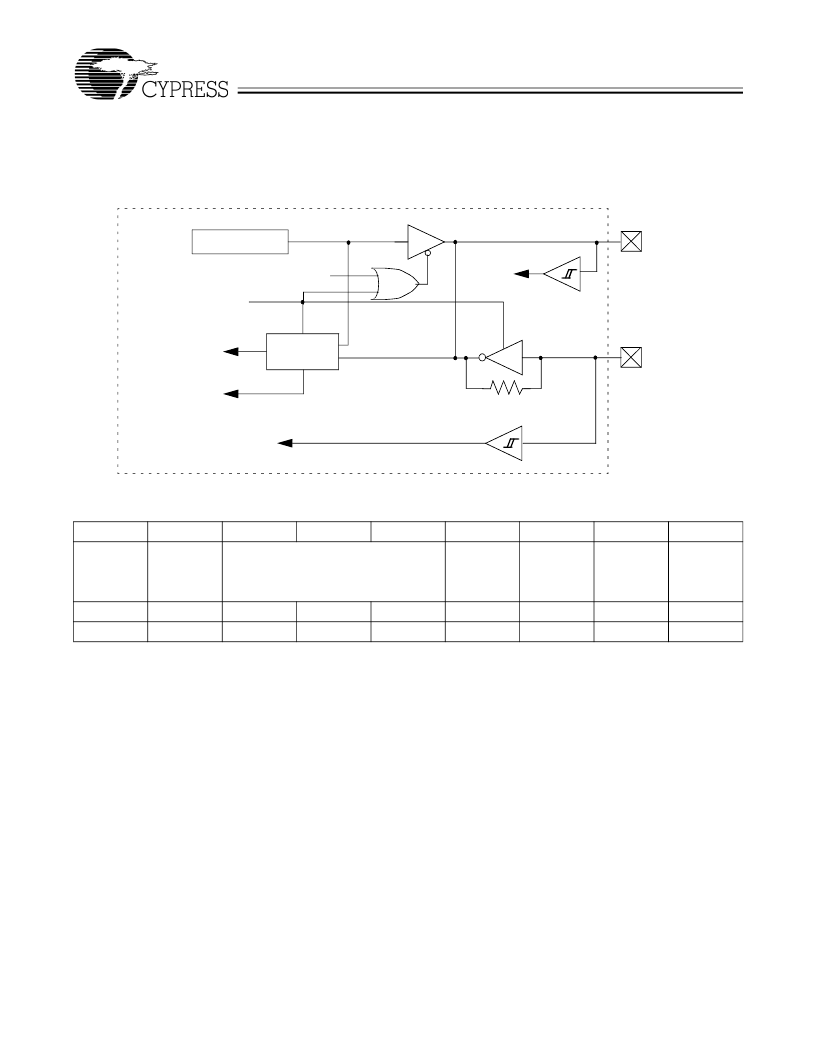
The chip can be clocked from either the internal on-chip clock, or from an oscillator based on an external resonator/crystal, as
shown in
Figure 9-1
. No additional capacitance is included on chip at the XTALIN/OUT pins. Operation is controlled by the Clock
Configuration Register,
Figure 9-2
.
Bit 7: Ext. Clock Resume Delay
External Clock Resume Delay bit selects the delay time when switching to the external oscillator from the internal oscillator
mode, or when waking from suspend mode with the external oscillator enabled.
1 = 4 ms delay.
0 = 128
μ
s delay.
The delay gives the oscillator time to start up. The shorter time is adequate for operation with ceramic resonators, while the
longer time is preferred for start-up with a crystal. (These times
do not include
an initial oscillator start-up time which depends
on the resonating element. This time is typically 50
–
100
μ
s for ceramic resonators and 1
–
10 ms for crystals). Note that this
bit only selects the delay time for the external clock mode. When waking from suspend mode with the internal oscillator (Bit 0
is LOW), the delay time is only 8
μ
s in addition to a delay of approximately 1
μ
s for the oscillator to start.
Bit [6:4]: Wake-up Timer Adjust Bit [2:0]
The Wake-up Timer Adjust Bits are used to adjust the Wake-up timer period.
If the Wake-up interrupt is enabled in the Global Interrupt Enable Register, the microcontroller will generate wake-up interrupts
periodically. The frequency of these periodical wake-up interrupts is adjusted by setting the Wake-up Timer Adjust Bit [2:0],
as described in Section 11.2. One common use of the wake-up interrupts is to generate periodical wake-up events during
suspend mode to check for changes, such as looking for movement in a mouse, while maintaining a low average power.
Bit 3: Low-voltage Reset Disable
When V
CC
drops below V
LVR
(see Section 23.0 for the value of V
LVR
) and the Low-voltage Reset circuit is enabled, the
microcontroller enters a partial suspend state for a period of t
START
(see Section 24.0 for the value of t
START
). Program
Figure 9-1. Clock Oscillator On-chip Circuit
Bit #
Bit Name
7
6
Wake-up Timer Adjust Bit [2:0]
5
4
2
1
0
Ext. Clock
Resume
Delay
Low-voltage
Reset
Disable
Precision
USB
Clocking
Enable
R/W
0
Internal
Clock
Output
Disable
R/W
0
External
Oscillator
Enable
Read/Write
Reset
R/W
0
R/W
0
R/W
0
R/W
0
R/W
0
R/W
0
Figure 9-2. Clock Configuration Register (Address 0xF8)
XTALOUT
XTALIN
Clk2x (12 MHz)
(to Microcontroller)
Clock
Doubler
Clk1x (6 MHz)
(to USB SIE)
Port 2.1
Ext Osc Enable
Port 2.2
Int Clk Output Disable
Internal Osc
相關(guān)PDF資料 |
PDF描述 |
|---|---|
| CY7C63231A-SC | enCoRe USB Low-speed USB Peripheral Controller |
| CY7C63221A | enCoRe USB Low-speed USB Peripheral Controller |
| CY7C63221A-PC | enCoRe USB Low-speed USB Peripheral Controller |
| CY7C63221A-XC | TV 32C 32#20 SKT RECP |
| CY7C63231A | enCoRe USB Low-speed USB Peripheral Controller(enCoRe USB 低速USB外設(shè)控制器) |
相關(guān)代理商/技術(shù)參數(shù) |
參數(shù)描述 |
|---|---|
| CY7C63310-PXC | 功能描述:USB 接口集成電路 USB 3K Flash 128 byte RAM COM RoHS:否 制造商:Cypress Semiconductor 產(chǎn)品:USB 2.0 數(shù)據(jù)速率: 接口類型:SPI 工作電源電壓:3.15 V to 3.45 V 工作電源電流: 最大工作溫度:+ 85 C 安裝風(fēng)格:SMD/SMT 封裝 / 箱體:WLCSP-20 |
| CY7C63310-SXC | 功能描述:USB 接口集成電路 USB Peripheral Cntrl 3K/128 16-SOIC RoHS:否 制造商:Cypress Semiconductor 產(chǎn)品:USB 2.0 數(shù)據(jù)速率: 接口類型:SPI 工作電源電壓:3.15 V to 3.45 V 工作電源電流: 最大工作溫度:+ 85 C 安裝風(fēng)格:SMD/SMT 封裝 / 箱體:WLCSP-20 |
| CY7C63310-SXCES | 制造商:Cypress Semiconductor 功能描述: |
| CY7C634121C-PVXC | 制造商:Cypress Semiconductor 功能描述: |
| CY7C634121C-PXC | 制造商:Cypress Semiconductor 功能描述: |
發(fā)布緊急采購(gòu),3分鐘左右您將得到回復(fù)。