- 您現(xiàn)在的位置:買賣IC網(wǎng) > PDF目錄379094 > CY7C43636 (Cypress Semiconductor Corp.) 512 x36/x18x2 Tri Bus FIFO(512 x36/x18x2 三路總線 先進先出) PDF資料下載
參數(shù)資料
| 型號: | CY7C43636 |
| 廠商: | Cypress Semiconductor Corp. |
| 英文描述: | 512 x36/x18x2 Tri Bus FIFO(512 x36/x18x2 三路總線 先進先出) |
| 中文描述: | 512 x36/x18x2三總線的FIFO(512 x36/x18x2三路總線先進先出) |
| 文件頁數(shù): | 8/40頁 |
| 文件大?。?/td> | 577K |
| 代理商: | CY7C43636 |
第1頁第2頁第3頁第4頁第5頁第6頁第7頁當前第8頁第9頁第10頁第11頁第12頁第13頁第14頁第15頁第16頁第17頁第18頁第19頁第20頁第21頁第22頁第23頁第24頁第25頁第26頁第27頁第28頁第29頁第30頁第31頁第32頁第33頁第34頁第35頁第36頁第37頁第38頁第39頁第40頁
CY7C43626
CY7C43636/CY7C43646
CY7C43666/CY7C43686
8
PRELIMINARY
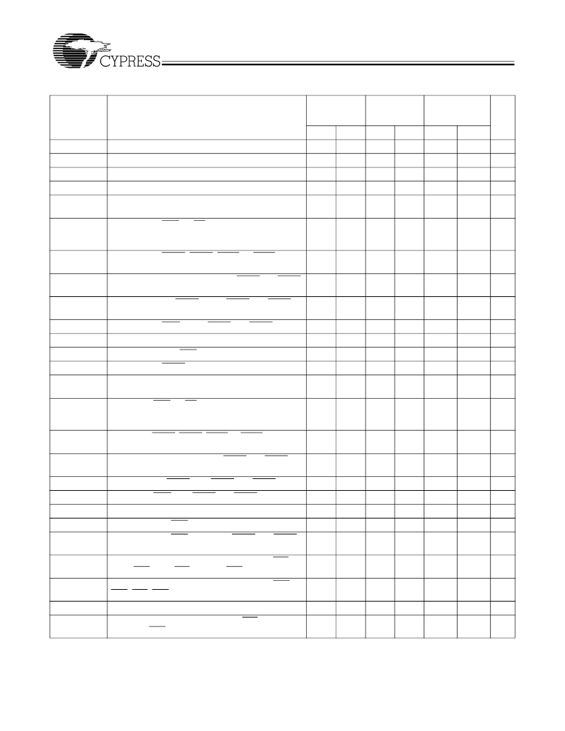
Switching Characteristics
Over the Operating Range
Parameter
Description
7C43626/
36/46/66/86
-7
7C43626/
36/46/66/86
-10
7C43626/
36/46/66/86
-15
Unit
Min.
Max.
Min.
Max.
Min.
Max.
f
S
t
CLK
t
CLKH
t
CLKL
Clock Frequency, CLKA,CLKB, or CLKC
133
100
67
MHz
Clock Cycle Time, CLKA,CLKB, or CLKC
7.5
10
15
ns
Pulse Duration, CLKA,CLKB, or CLKC HIGH
3.5
4
6
ns
Pulse Duration, CLKA,CLKB, or CLKC LOW
Set-Up Time, A
0
–
35
before CLKA
↑
B
0
–
17
before
CLKB
↑,
and C
0
–
17
before CLKC
↑
Set-Up Time, CSA, W/RA, ENA, and MBA before
CLKA
↑
; RENB and MBB before CLKB
↑
and WENC
and MBC before CLKC
↑
Set-Up Time, MRS1, MRS2, PRS1, or PRS2 LOW
before CLKA
↑
or CLKB
↑
[7]
Set-Up Time, FS0 and FS1 before MRS1 and MRS2
HIGH
3.5
4
6
ns
t
DS
3
4
5
ns
t
ENS
3
4
5
ns
t
RSTS
2.5
4
5
ns
t
FSS
5
7
7.5
ns
t
BES
t
SPMS
t
SDS
t
SENS
t
FWS
Set-Up Time, BE/FWFT before MRS1 and MRS2
HIGH
5
7
7.5
ns
Set-Up Time, SPM before MRS1 and MRS2 HIGH
Set-Up Time, FS0/SD before CLKA
↑
Set-Up Time, FS1/SEN before CLKA
↑
Set-Up Time, FWFT before CLKA
↑
Hold Time, A
0
–
35
before CLKA
↑
B
0
–
17
before CLKB
↑,
and C
0
–
17
before CLKC
↑
Hold Time, CSA, W/RA, ENA, and MBA before
CLKA
↑
RENB and MBB before CLKB
↑
and WENC
and MBC before CLKC
↑
Hold Time, MRS1, MRS2, PRS1, or PRS2 LOW after
CLKA
↑
or CLKB
↑
[7]
Hold Time, FS0 and FS1 after MRS1 and MRS2
HIGH
5
7
7.5
ns
3
4
5
ns
3
4
5
ns
0
0
0
ns
t
DH
0
0
0
ns
t
ENH
0
0
0
ns
t
RSTH
1
2
4
ns
t
FSH
t
BEH
t
SPMH
t
SDH
t
SENH
1
1
2
ns
Hold Time, BE/FWFT after MRS1 and MRS2 HIGH
1
1
2
ns
Hold Time, SPM after MRS1 and MRS2 HIGH
Hold Time, FS0/SD after CLKA
↑
Hold Time, FS1/SEN after CLKA
↑
Hold Time, FS1/SEN HIGH after MRS1 and MRS2
HIGH
Skew Time between CLKA
↑
and CLKB
↑
for EFA/
ORA, EFB/ORB, FFA/IRA, and FFC/IRC
Skew Time between CLKA
↑
and CLKB
↑
for AEA,
AEB, AFA, AFC
Access Time, CLKA
↑
to A
0
–
35
and CLKB
↑
to B
0
–
17
Propagation Delay Time, CLKA
↑
to FFA/IRA and
CLKB
↑
to FFC/IRC
1
1
2
ns
0
0
0
ns
0
0
0
ns
t
SPH
0
1
2
ns
t
SKEW1[8]
5
5
7.5
ns
t
SKEW2[8]
t
A
7
8
12
ns
1
6
1
8
3
10
ns
t
WFF
Notes:
7.
8.
1
6
1
8
2
8
ns
Requirement to count the clock edge as one of at least four needed to reset a FIFO.
Skew time is not a timing constraint for proper device operation and is only included to illustrate the timing relationship between CLKA cycle and CLKB cycle.
相關(guān)PDF資料 |
PDF描述 |
|---|---|
| CY7C43626 | 256 x36/x18x2 Tri Bus FIFO(256 x36/x18x2 三路總線先進先出) |
| CY7C43646 | 1K x36/x18x2 Tri Bus FIFO(1K x36/x18x2 三路總線 先進先出) |
| CY7C43666 | 4K x36/x18x2 Tri Bus FIFO(4K x36/x18x2 三路總線先進先出) |
| CY7C43686 | 16K x36/x18x2 Tri Bus FIFO(16K x36/x18x2 三路總線先進先出) |
| CY7C43662AV | 3.3V 4K x36 x2 Bidirectional Synchronous FIFO(3.3V 4K x36 x2 雙向同步先進先出) |
相關(guān)代理商/技術(shù)參數(shù) |
參數(shù)描述 |
|---|---|
| CY7C43642-10AC | 制造商:Cypress Semiconductor 功能描述:FIFO Mem Sync Dual Depth/Width Bi-Dir 1K x 36 x 2 120-Pin TQFP |
| CY7C43643-15AC | 制造商:Cypress Semiconductor 功能描述:FIFO Mem Sync Dual Depth/Width Uni-Dir 1K x 36 128-Pin TQFP 制造商:Rochester Electronics LLC 功能描述:- Bulk |
| CY7C43643AV-10AC | 制造商:Cypress Semiconductor 功能描述:FIFO Mem Sync Dual Depth/Width Uni-Dir 1K x 36 128-Pin TQFP |
| CY7C43643AV-15AC | 制造商:Cypress Semiconductor 功能描述:FIFO Mem Sync Dual Depth/Width Uni-Dir 1K x 36 128-Pin TQFP |
| CY7C43643AV-7AC | 制造商:Cypress Semiconductor 功能描述:FIFO Mem Sync Dual Depth/Width Uni-Dir 1K x 36 128-Pin TQFP |
發(fā)布緊急采購,3分鐘左右您將得到回復(fù)。