- 您現(xiàn)在的位置:買賣IC網(wǎng) > PDF目錄379090 > CY7C1992BV18 (Cypress Semiconductor Corp.) 18-Mbit DDR-II SIO SRAM 2-Word(2字Burst結(jié)構(gòu),18-Mbit DDR-II SIO SRAM) PDF資料下載
參數(shù)資料
| 型號(hào): | CY7C1992BV18 |
| 廠商: | Cypress Semiconductor Corp. |
| 英文描述: | 18-Mbit DDR-II SIO SRAM 2-Word(2字Burst結(jié)構(gòu),18-Mbit DDR-II SIO SRAM) |
| 中文描述: | 18兆位的DDR - II二氧化硅的SRAM 2字(2字突發(fā)結(jié)構(gòu),18 -兆位的DDR - II二氧化硅的SRAM) |
| 文件頁數(shù): | 9/25頁 |
| 文件大?。?/td> | 1031K |
| 代理商: | CY7C1992BV18 |
CY7C1392BV18
CY7C1992BV18
CY7C1393BV18
CY7C1394BV18
Document Number: 38-05623 Rev. *B
Page 9 of 25
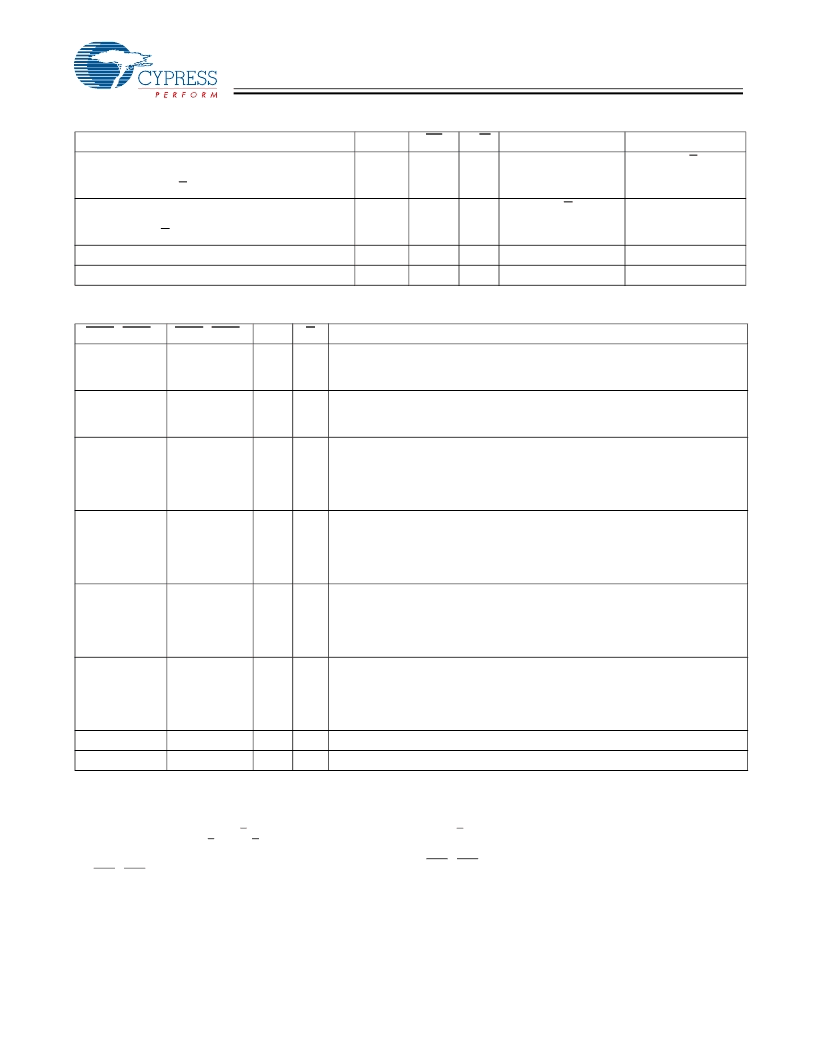
Truth Table
[2, 3, 4, 5, 6, 7]
Operation
K
LD
L
R/W
L
DQ
DQ
Write Cycle:
Load address; wait one cycle; input write data on
consecutive K and K rising edges.
Read Cycle:
Load address; wait one and a half cycle; read data
on consecutive C and C rising edges.
NOP: No Operation
Standby: Clock Stopped
L-H
D(A + 0) at K(t + 1)
↑
D(A + 1) at K(t + 1)
↑
L-H
L
H
Q(A + 0) at C(t + 1)
↑
Q(A + 1) at C(t + 2)
↑
L-H
H
X
X
X
High-Z
Previous State
High-Z
Previous State
Stopped
Write Cycle Descriptions
(CY7C1392BV18 and CY7C1393BV18)
[2, 8]
BWS
0
/NWS
0
L
BWS
1
/NWS
1
L
K
K
-
Comments
L-H
During the Data portion of a Write sequence
:
CY7C1392BV18
both nibbles (D
[7:0]
) are written into the device,
CY7C1393BV18
both bytes (D
[17:0]
) are written into the device.
L-H During the Data portion of a Write sequence
:
CY7C1392BV18
both nibbles (D
[7:0]
) are written into the device,
CY7C1393BV18
both bytes (D
[17:0]
) are written into the device.
-
During the Data portion of a Write sequence
:
CY7C1392BV18
only the lower nibble (D
[3:0]
) is written into the device. D
[7:4]
will remain unaltered,
CY7C1393BV18
only the lower byte (D
[8:0]
) is written into the device. D
[17:9]
will remain unaltered.
L-H During the Data portion of a Write sequence
:
CY7C1392BV18
only the lower nibble (D
[3:0]
) is written into the device. D
[7:4]
will remain unaltered,
CY7C1393BV18
only the lower byte (D
[8:0]
) is written into the device. D
[17:9]
will remain unaltered.
–
During the Data portion of a Write sequence
:
CY7C1392BV18
only the upper nibble (D
[7:4]
) is written into the device. D
[3:0]
will remain unaltered,
CY7C1393BV18
only the upper byte (D
[17:9]
) is written into the device. D
[8:0]
will remain unaltered.
L-H During the Data portion of a Write sequence
:
CY7C1392BV18
only the upper nibble (D
[7:4]
) is written into the device. D
[3:0]
will remain unaltered,
CY7C1393BV18
only the upper byte (D
[17:9]
) is written into the device. D
[8:0]
will remain unaltered.
–
No data is written into the devices during this portion of a Write operation.
L-H No data is written into the devices during this portion of a Write operation.
L
L
-
L
H
L-H
L
H
-
H
L
L-H
H
L
–
H
H
H
H
L-H
–
Notes:
2. X = “Don't Care,” H = Logic HIGH, L = Logic LOW,
↑
represents rising edge.
3. Device will power-up deselected and the outputs in a tri-state condition.
4. “A” represents address location latched by the devices when transaction was initiated. A + 0, A + 1 represents the internal address sequence in the burst.
5. “t” represents the cycle at which a Read/Write operation is started. t+1, t + 2 and t +3 are the first, second and third clock cycles succeeding the “t” clock cycle.
6. Data inputs are registered at K and K rising edges. Data outputs are delivered on C and C rising edges, except when in single clock mode.
7. It is recommended that K = K and C = C = HIGH when clock is stopped. This is not essential, but permits most rapid restart by overcoming transmission line
charging symmetrically.
8. Assumes a Write cycle was initiated per the Write Cycle Description Truth Table. BWS
, BWS
in the case of CY7C1392BV18 and CY7C1393BV18 and also
BWS
2
, BWS
3
in the case of CY7C1394BV18 can be altered on different portions of a write cycle, as long as the set-up and hold requirements are achieved.
相關(guān)PDF資料 |
PDF描述 |
|---|---|
| CY7C199 | 32K x 8 Static RAM(32K x 8靜態(tài) RAM) |
| CY7C271A-35PC | 32K x 8 Power Switched and Reprogrammable PROM |
| CY7C271A-25JC | Box-shaped pin header, Discrete wire crimping connection, Complete locking mechanism, Discrete wire connectors; HRS No: 541-0971-6 00; No. of Positions: 2; Operating Temperature Range (degrees C): -35 to 85; General Description: Accessory; Retainer |
| CY7C271A-30PC | Box-shaped pin header, Discrete wire crimping connection, Complete locking mechanism, Discrete wire connectors; HRS No: 541-0811-0 00; No. of Positions: 2; Connector Type: Wire; Contact Gender: Female; Contact Spacing (mm): 2.5; Terminal Pitch (mm): 2.5; Current Rating(Amps)(Max.): 3; Operating Temperature Range (degrees C): -35 to 85; General Description: Housing; Crimping |
| CY7C271A | 32K x 8 Power Switched and Reprogrammable PROM(32K x 8功率轉(zhuǎn)換和 可重復(fù)編程的 PROM) |
相關(guān)代理商/技術(shù)參數(shù) |
參數(shù)描述 |
|---|---|
| CY7C19930VC | 制造商:CYPRESS 功能描述:* |
| CY7C19935DC | 制造商:CSC 功能描述: |
| CY7C199-35DMB | 制造商:Cypress Semiconductor 功能描述:SRAM Chip Async Single 5V 256K-Bit 32K x 8 35ns 28-Pin CDIP |
| CY7C199-35LMB | 制造商:Cypress Semiconductor 功能描述:SRAM Chip Async Single 5V 256K-Bit 32K x 8 35ns 28-Pin LCC |
| CY7C19935PC | 制造商:CYPRESS 功能描述:* |
發(fā)布緊急采購,3分鐘左右您將得到回復(fù)。