- 您現(xiàn)在的位置:買賣IC網(wǎng) > PDF目錄379008 > CY2CC1910SIT (CYPRESS SEMICONDUCTOR CORP) 1:10 Clock Fanout Buffer with Output Enable PDF資料下載
參數(shù)資料
| 型號(hào): | CY2CC1910SIT |
| 廠商: | CYPRESS SEMICONDUCTOR CORP |
| 元件分類: | 時(shí)鐘及定時(shí) |
| 英文描述: | 1:10 Clock Fanout Buffer with Output Enable |
| 中文描述: | LOW SKEW CLOCK DRIVER, 10 TRUE OUTPUT(S), 0 INVERTED OUTPUT(S), PDSO24 |
| 封裝: | 0.300 INCH, SOIC-24 |
| 文件頁數(shù): | 2/8頁 |
| 文件大小: | 129K |
| 代理商: | CY2CC1910SIT |
COMLINK
SERIES
CY2CC1910
Document #: 38-07347 Rev. *B
Page 2 of 8
Maximum Ratings
[1,2]
Storage Temperature: ................................
–
65
°
C to + 150
°
C
Ambient Temperature:...................................
–
40
°
C to +85
°
C
Supply Voltage to Ground Potential
V
CC
..................................................................
–
0.5V to 4.6V
Input.................................................................
–
0.5V to 5.8V
Variable Output Impedance Control (VOI
)
Supply Voltage to Ground Potential
(Outputs only)...........................................
–
0.5V to V
DD
+ 1V
DC Output Voltage....................................
–
0.5V to V
DD
+ 1V
Power Dissipation........................................................0.75W
DC Electrical Characteristics
@ 3.3V (see
Figure 2
)
Parameter
V
OH
V
OL
V
IH
V
IL
I
IH
I
IL
I
I
V
IK
I
OK
O
OFF
V
H
DC Electrical Characteristics
@ 2.5V (see
Figure 2
)
Description
Conditions
Min.
2.3
Typ.
3.3
0.2
Max.
Unit
V
V
V
V
uA
uA
uA
V
mA
uA
mV
Output High Voltage
Output Low Voltage
Input High Voltage
Input Low Voltage
Input High Current
Input Low Current
Input High Current
Clamp Diode Voltage
Continuous Clamp Current
Power-down Disable
Input Hysteresis
V
DD
= Min.,V
IN
= V
IH
or V
IL
V
DD
= Min.,V
IN
= V
IH
or V
IL
Guaranteed Logic High Level
Guaranteed Logic Low Level
V
DD
= Max.
V
DD
= Max.
V
DD
= Max.,V
IN
= V
DD
(Max.)
V
DD
= Min., I
IN
=
–
18 mA
V
DD
= Max.,V
OUT
= GND
V
DD
= GND,V
OUT
= < 4.5V
I
OH
=
–
12 mA
I
OL
= 12 mA
0.5
5.8
0.8
1
–
1
20
–
1.2
–
50
100
2
V
IN
= 2.7V
V
IN
= 0.5V
–
0.7
80
Parameter
Description
Conditions
Min.
1.8
1.6
Typ.
Max.
Unit
V
V
V
V
V
uA
uA
uA
V
mA
uA
mV
V
OH
Output High Voltage
V
DD
= Min.,V
IN
= V
IH
or V
IL
V
DD
= Min.,V
IN
= V
IH
or V
IL
Guaranteed Logic High Level
Guaranteed Logic Low Level
V
DD
= Max.
V
DD
= Max.
V
DD
= Max.,V
IN
= V
DD
(Max.)
V
DD
= Min., I
IN
=
–
18 mA
V
DD
= Max.,V
OUT
= GND
V
DD
= GND, V
OUT
= < 4.5V
V
DD
= Min.,V
IN
= V
IH
or V
IL
I
OH
=
–
7 mA
I
OH
= 12 mA
I
OL
= 12 mA
V
OL
V
IH
V
IL
I
IH
I
IL
I
I
V
IK
I
OK
O
OFF
V
H
Note:
1.
2.
Output Low Voltage
Input High Voltage
Input Low Voltage
Input High Current
Input Low Current
Input High Current
Clamp Diode Voltage
Continuous Clamp Current
Power-down Disable
Input Hysteresis
0.65
5.0
0.8
1
–
1
20
–
1.2
–
50
100
1.6
V
IN
= 2.4V
V
IN
= 0.5V
–
0.7
80
Multiple Supplies:
The Voltage on any input or I/O pin cannot exceed the power pin during power-up. Power supply sequencing is NOT required.
Stresses greater than those listed under absolute maximum ratings may cause permanent damage to the device. This is intended to be a stress rating only
and functional operation of the device at these or any other conditions above those indicated in the operation sections of this specification is not implied.
Exposure to absolute maximum rating conditions for extended periods may affect reliability.
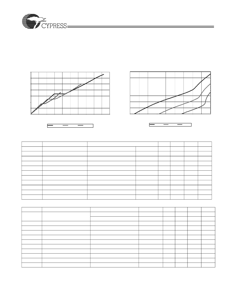
Pull Down
0
0.5
1
1.5
2
2.5
3
3.5
0
0.01
0.02
0.03
0.04
0.05
0.06
0.07
0.08
0.09
0.1
Iol (A)
Vdd = 3.3 V
Vdd = 2.5 V
Vdd = 1.8 V
Pull Up
0
0.5
1
1.5
2
2.5
3
3.5
-0.18
-0.16
-0.14
-0.12
-0.1
-0.08
-0.06
-0.04
-0.02
0
Ioh (A)
Vdd = 3.3 V
Vdd = 2.5 V
Vdd = 1.8 V
Figure 1. Output Voltage vs. Output Current (T
A
= 25
°
C)
相關(guān)PDF資料 |
PDF描述 |
|---|---|
| CY2DP814SC | 1:4 Clock Fanout Buffer |
| CY2DP814ZC | DB37 INTERFACE DATA CBL DB37 Male - DB37 Female |
| CY2DP814ZCT | DB37 INTERFACE DATA CBL DB37 Male - DB37 Female |
| CY2DP814 | 1:4 Clock Fanout Buffer |
| CY2DP814SCT | 1:4 Clock Fanout Buffer |
相關(guān)代理商/技術(shù)參數(shù) |
參數(shù)描述 |
|---|---|
| CY2CC810 | 制造商:CYPRESS 制造商全稱:Cypress Semiconductor 功能描述:1:10 Clock Fanout Buffer |
| CY2CC810_06 | 制造商:CYPRESS 制造商全稱:Cypress Semiconductor 功能描述:1:10 Clock Fanout Buffer |
| CY2CC8100I | 制造商:Cypress Semiconductor 功能描述: |
| CY2CC8100XC-1 | 制造商:Cypress Semiconductor 功能描述: |
| CY2CC8100XI | 制造商:Cypress Semiconductor 功能描述: |
發(fā)布緊急采購,3分鐘左右您將得到回復(fù)。