- 您現(xiàn)在的位置:買賣IC網(wǎng) > PDF目錄379006 > CY28347ZC (CYPRESS SEMICONDUCTOR CORP) Universal Single-chip Clock Solution for VIA P4M266/KM266 DDR Systems PDF資料下載
參數(shù)資料
| 型號: | CY28347ZC |
| 廠商: | CYPRESS SEMICONDUCTOR CORP |
| 元件分類: | XO, clock |
| 英文描述: | Universal Single-chip Clock Solution for VIA P4M266/KM266 DDR Systems |
| 中文描述: | 200 MHz, PROC SPECIFIC CLOCK GENERATOR, PDSO56 |
| 封裝: | 6 X 14 MM, TSSOP-56 |
| 文件頁數(shù): | 9/22頁 |
| 文件大小: | 188K |
| 代理商: | CY28347ZC |
CY28347
Document #: 38-07352 Rev. *C
Page 9 of 22
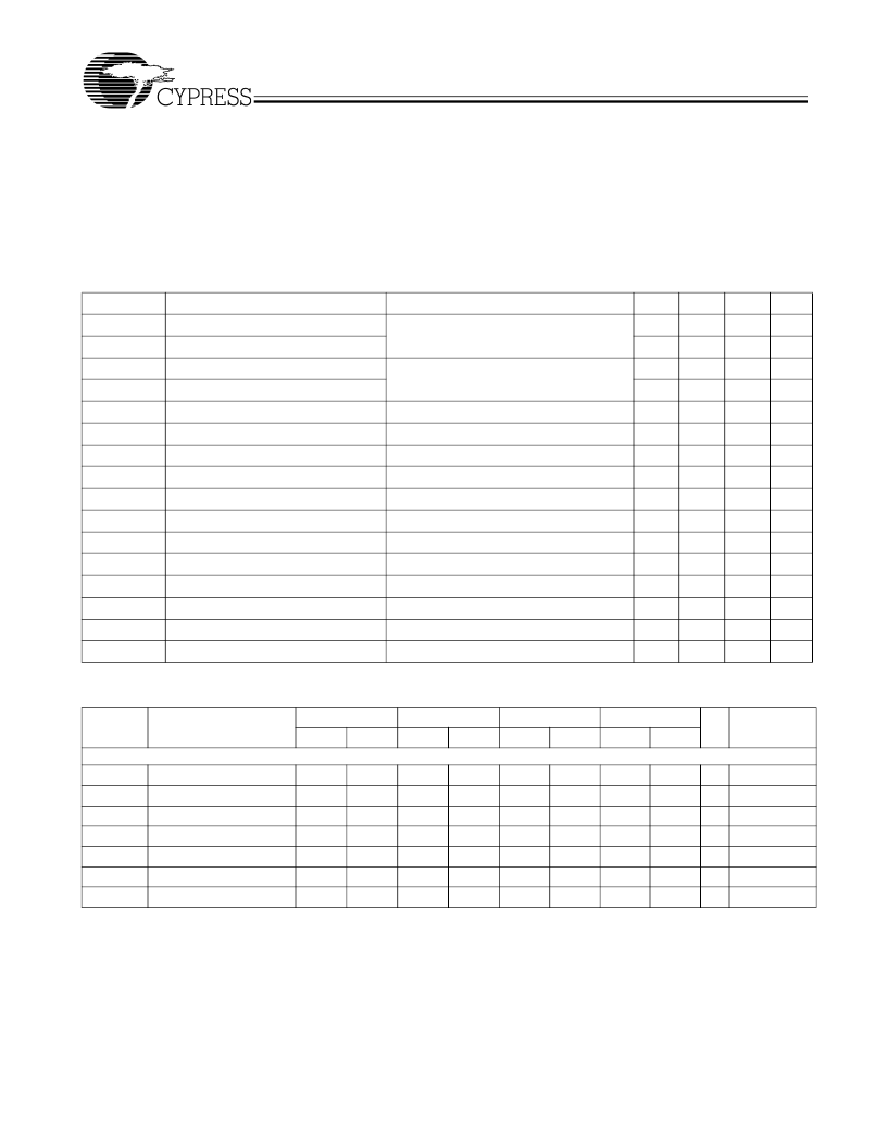
Maximum Ratings
[3]
Input Voltage Relative to V
SS
:.............................. V
SS
–
0.3V
Input Voltage Relative to V
DDQ
or AV
DD
: .............V
DD
+ 0.3V
Storage Temperature: ................................
–
65
°
C to + 150
°
C
Operating Temperature:....................................0
°
C to +70
°
C
Maximum ESD.............................................................2000V
Maximum Power Supply: ................................................5.5V
This device contains circuitry to protect the inputs against
damage due to HIGH static voltages or electric field. However,
precautions should be take to avoid application of any voltage
higher than the maximum rated voltages to this circuit. For
proper operation, V
IN
and V
OUT
should be constrained to the
range.
V
SS
< (V
IN
or V
OUT
) < V
DD
Unused inputs must always be tied to an appropriate logic
voltage level (either V
SS
or V
DD
).
DC Parameters
(V
DD
= V
DDPCI
= V
DDAGP
= V
DDR
= V
DD48M
= V
DDC
= 3.3V ± 5%, V
DDI
= V
DD
= 2.5 ± 5%, T
A
= 0
°
C to +70
°
C)
Parameter
VIL1
VIH1
VIL2
VIH2
Vol
Iol
Ioz
Idd3.3V
Idd2.5V
Ipd
Ipup
Ipdwn
Cin
Cout
Lpin
Cxtal
Description
Conditions
Min.
Typ.
Max.
1.0
Unit
Vdc
Vdc
Vdc
Vdc
V
mA
μ
A
mA
mA
mA
μ
A
μ
A
pF
pF
pF
pF
Input LOW Voltage
Input HIGH Voltage
Input LOW Voltage
Input HIGH Voltage
Output LOW Voltage for Sreset#
Pull-down Current for Sreset#
Three-state Leakage Current
Dynamic Supply Current
Dynamic Supply Current
Power-down Supply current
Internal Pull-up Device Current
Internal Pull-down Device Current
Input Pin Capacitance
Output Pin Capacitance
Pin Inductance
Crystal Pin Capacitance
Applicable to PD#, F S(0:4)
2.0
Applicable to SDATA and SCLK
1.0
2.2
0.4
24
IOL
VOL = 0.4V
35
10
180
200
4.0
–
25
10
5
6
7
45
CPU frequency set at 133.3
[4]
CPU frequency set at 133.3 MHz
[4]
PD# = 0
Input @ V
SS
Input @ V
DD
156
177
3.8
Measured from the X
IN
or X
OUT
to V
SS
27
36
AC Parameters
Parameter
Crystal
TDC
TPeriod
VHIGH
VLOW
Tr / Tf
TCCJ
Txs
Description
66 MHz
Min.
100 MHz
Min.
133 MHz
Min.
200 MHz
Min.
Unit
Notes
Max.
Max.
Max.
Max.
Xin Duty Cycle
Xin Period
Xin HIGH Voltage
Xin LOW Voltage
Xin Rise and Fall Times
Xin Cycle to Cycle Jitter
Crystal Start-up Time
45
55
71.0
V
DD
0.3V
DD
10.0
500
30
45
55
71.0
V
DD
0.3V
DD
10.0
500
30
45
55
71.0
V
DD
0.3V
DD
10
500
30
45
55
71.0
V
DD
0.3V
DD
10
500
30
% 5,6,7,8
ns 5,6,7,8
V 7,9
V
ns 7
ps 10,11,12,13
ms 9
69.84
0.7V
DD
0
69.84
0.7V
DD
0
69.84
0.7V
DD
0
69.84
0.7V
DD
0
Notes:
3.
4.
5.
6.
7.
Multiple Supplies:
The Voltage on any input or I/O pin cannot exceed the power pin during power-up. Power supply sequencing is NOT required.
All outputs loaded as per maximum capacitative load table in P4 and DDR mode.
See
Table 11
.
All outputs loaded as per loading specified in the loading table. See
Table 11
.
This measurement is applicable with Spread ON or spread OFF.
This is required for the duty cycle on the REF clock out to be as specified. The device will operate reliably with input duty cycles up to 30/70 but the REF clock
duty cycle will not be within data sheet specifications.
The typical value of VX is expected to be 0.5*VDDD (or 0.5*VDDC for CPUCS signals) and will track the variations in the DC level of the same.
Measured between 0.2Vdd and 0.7Vdd.
9.
between 20% and 80% for differential signals.
11.
Probes are placed on the pins, and measurements are acquired at 2.4V for 3.3V signals and at 2.0V for 2.5V signals.
12. When Xin is driven from and external clock source (3.3V parameters apply).
13. When Crystal meets minimum 40 ohm device series resistance specification.
8.
相關(guān)PDF資料 |
PDF描述 |
|---|---|
| CY28347ZCT | Universal Single-chip Clock Solution for VIA P4M266/KM266 DDR Systems |
| CY28347OC | Universal Single-chip Clock Solution for VIA P4M266/KM266 DDR Systems |
| CY28347OCT | Universal Single-chip Clock Solution for VIA P4M266/KM266 DDR Systems |
| CY28349B | FTG for Intel Pentium 4 CPU and Chipsets |
| CY28349BOC | FTG for Intel Pentium 4 CPU and Chipsets |
相關(guān)代理商/技術(shù)參數(shù) |
參數(shù)描述 |
|---|---|
| CY28347ZCT | 制造商:Rochester Electronics LLC 功能描述:FTG FOR VIA P4 CHIPSET - Tape and Reel |
| CY28349 | 制造商:SPECTRALINEAR 制造商全稱:SPECTRALINEAR 功能描述:FTG for Intel㈢ Pentium㈢ 4 CPU and Chipsets |
| CY28349B | 制造商:SPECTRALINEAR 制造商全稱:SPECTRALINEAR 功能描述:FTG for Intel㈢ Pentium㈢ 4 CPU and Chipsets |
| CY28349B_05 | 制造商:CYPRESS 制造商全稱:Cypress Semiconductor 功能描述:FTG for Intel㈢ Pentium㈢ 4 CPU and Chipsets |
| CY28349BOC | 制造商:Rochester Electronics LLC 功能描述:- Bulk |
發(fā)布緊急采購,3分鐘左右您將得到回復(fù)。