- 您現(xiàn)在的位置:買賣IC網(wǎng) > PDF目錄42903 > ATF-521P8-TR2 L BAND, Si, N-CHANNEL, RF SMALL SIGNAL, HEMFET, MO-229 PDF資料下載
參數(shù)資料
| 型號: | ATF-521P8-TR2 |
| 元件分類: | 小信號晶體管 |
| 英文描述: | L BAND, Si, N-CHANNEL, RF SMALL SIGNAL, HEMFET, MO-229 |
| 封裝: | 2 x 2 MM, 0.75 MM HEIGHT,LEAD FREE, PLASTIC,LPCC-8 |
| 文件頁數(shù): | 9/23頁 |
| 文件大?。?/td> | 319K |
| 代理商: | ATF-521P8-TR2 |
17
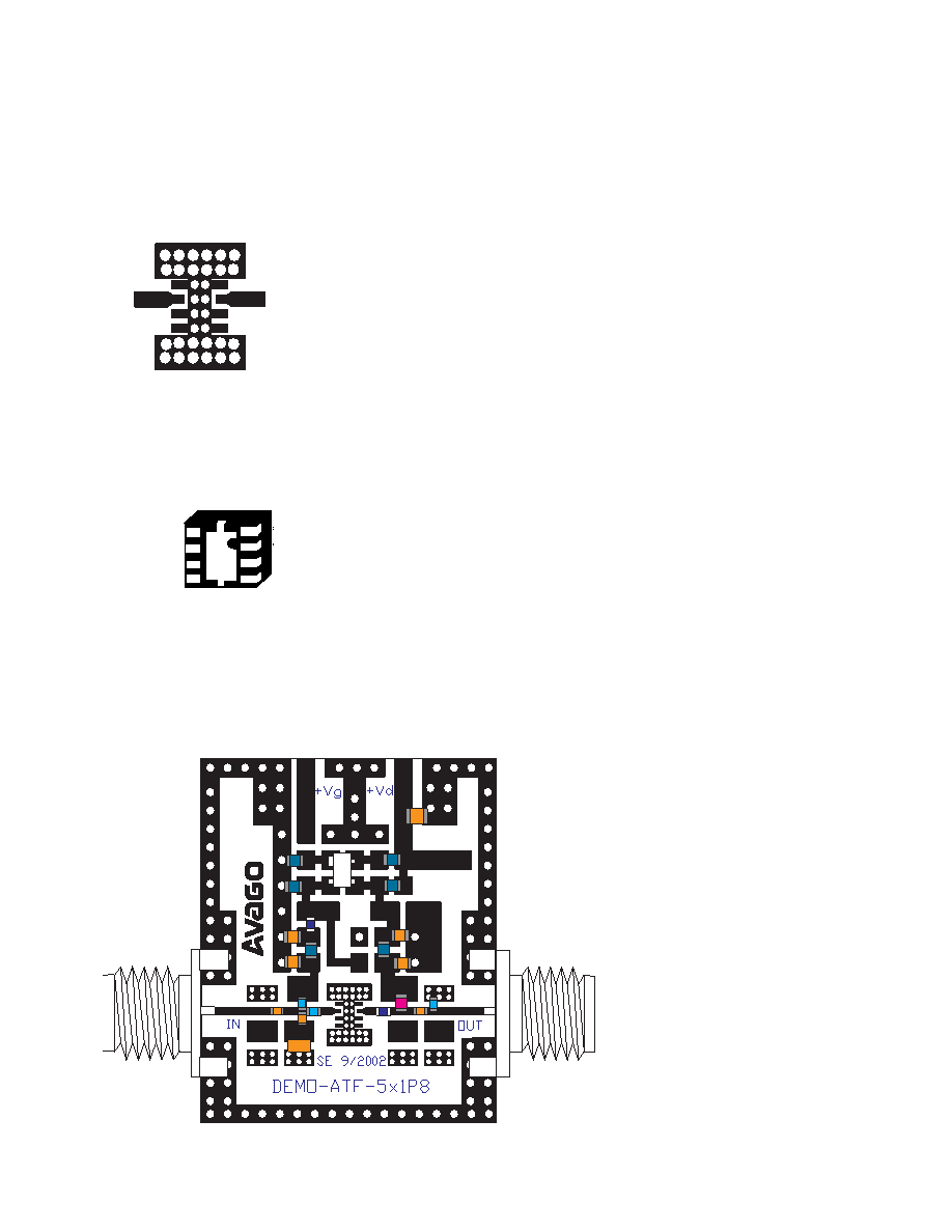
PCB Layout
A recommended PCB pad layout for the Leadless Plastic
Chip Carrier (LPCC) package used by the ATF521P8 is
shown in Figure 10. This layout provides plenty of plated
through hole vias for good thermal and RF grounding. It
also provides a good transition from microstrip to the
device package. For more detailed dimensions refer to
Section 9 of the data sheet.
This simplifies RF grounding by reducing the amount
of inductance from the source to ground. It is also
recommended to ground pins 1 and 4 since they are
also connected to the device source. Pins 3, 5, 6, and 8
are not connected, but may be used to help dissipate
heat from the package or for better alignment when
soldering the device.
This threelayer board (Figure 12) contains a 10mil layer
and a 52mil layer separated by a ground plane. The first
layer is Getek RG200D material with dielectric constant
of 3.8. The second layer is for mechanical rigidity and
consists of FR4 with dielectric constant of 4.2.
High Linearity Tx Driver
The need for higher data rates and increased voice
capacity gave rise to a new third generation standard
know as Wideband CDMA or UMTS. This new standard
requires higher performance from radio components
such as higher dynamic range and better linearity. For
example, a WCDMA waveform has a very high peak to
average ratio which forces amplifiers in a transmit chain
to have very good Adjacent Channel Leakage power
Ratio or ACLR, or else operate in a backed off mode.
If the amplifier is not backed off then the waveform is
compressed and the signal becomes very nonlinear.
This application example presents a highly linear
transmit drive for use in the 2.14GHz frequency range.
Using the RF matching techniques described earlier,
ATF521P8 is matched to the following input and output
impedances:
Figure 12. ATF-521P8 demoboard.
Pin 8
Source
(Thermal/RF
Gnd)
Pin 7 (Drain)
Pin 6
Pin 5
Pin 1 (Source)
Pin 2 (Gate)
Pin 3
Pin 4 (Source)
Bottom View
J1
J2
BCV62B
C1
C8
0
L3
R1
R2
R3
R4
R5
R6
L4
C2
C3
C5
C6
C4
C7
L2
L1
short
Figure 10. Microstripline Layout.
RF Grounding
Unlike SOT packages, ATF521P8 is housed in a leadless
package with the die mounted directly to the lead
frame or the belly of the package shown in Figure 11.
Figure 11. LPCC Package for ATF-521P8.
相關(guān)PDF資料 |
PDF描述 |
|---|---|
| ATF-521P8-TR1 | L BAND, Si, N-CHANNEL, RF SMALL SIGNAL, HEMFET, MO-229 |
| ATF-521P8-BLK | L BAND, Si, N-CHANNEL, RF SMALL SIGNAL, HEMFET, MO-229 |
| ATF-53189-TR1 | C BAND, Si, N-CHANNEL, RF SMALL SIGNAL, HEMFET |
| ATF-53189-BLK | C BAND, Si, N-CHANNEL, RF SMALL SIGNAL, HEMFET |
| ATF-531P8-BLK | C BAND, Si, N-CHANNEL, RF SMALL SIGNAL, HEMFET, MO-229 |
相關(guān)代理商/技術(shù)參數(shù) |
參數(shù)描述 |
|---|---|
| ATF524S16M | 制造商:n/a 功能描述:Inverter Semiconductor |
| ATF-53189 | 制造商:AGILENT 制造商全稱:AGILENT 功能描述:Enhancement Mode Pseudomorphic HEMT in SOT 89 Package |
| ATF-53189-BLK | 功能描述:射頻GaAs晶體管 Transistor GaAs High Linearity RoHS:否 制造商:TriQuint Semiconductor 技術(shù)類型:pHEMT 頻率:500 MHz to 3 GHz 增益:10 dB 噪聲系數(shù): 正向跨導(dǎo) gFS(最大值/最小值):4 S 漏源電壓 VDS: 閘/源擊穿電壓:- 8 V 漏極連續(xù)電流:3 A 最大工作溫度:+ 150 C 功率耗散:10 W 安裝風(fēng)格: 封裝 / 箱體: |
| ATF-53189-TR1 | 功能描述:射頻GaAs晶體管 Transistor GaAs High Linearity RoHS:否 制造商:TriQuint Semiconductor 技術(shù)類型:pHEMT 頻率:500 MHz to 3 GHz 增益:10 dB 噪聲系數(shù): 正向跨導(dǎo) gFS(最大值/最小值):4 S 漏源電壓 VDS: 閘/源擊穿電壓:- 8 V 漏極連續(xù)電流:3 A 最大工作溫度:+ 150 C 功率耗散:10 W 安裝風(fēng)格: 封裝 / 箱體: |
| ATF-53189-TR2 | 功能描述:射頻GaAs晶體管 Transistor GaAs Hi gh Linearity RoHS:否 制造商:TriQuint Semiconductor 技術(shù)類型:pHEMT 頻率:500 MHz to 3 GHz 增益:10 dB 噪聲系數(shù): 正向跨導(dǎo) gFS(最大值/最小值):4 S 漏源電壓 VDS: 閘/源擊穿電壓:- 8 V 漏極連續(xù)電流:3 A 最大工作溫度:+ 150 C 功率耗散:10 W 安裝風(fēng)格: 封裝 / 箱體: |
發(fā)布緊急采購,3分鐘左右您將得到回復(fù)。