- 您現(xiàn)在的位置:買賣IC網(wǎng) > PDF目錄42903 > ATF-521P8-TR2 L BAND, Si, N-CHANNEL, RF SMALL SIGNAL, HEMFET, MO-229 PDF資料下載
參數(shù)資料
| 型號(hào): | ATF-521P8-TR2 |
| 元件分類: | 小信號(hào)晶體管 |
| 英文描述: | L BAND, Si, N-CHANNEL, RF SMALL SIGNAL, HEMFET, MO-229 |
| 封裝: | 2 x 2 MM, 0.75 MM HEIGHT,LEAD FREE, PLASTIC,LPCC-8 |
| 文件頁(yè)數(shù): | 6/23頁(yè) |
| 文件大小: | 319K |
| 代理商: | ATF-521P8-TR2 |
第1頁(yè)第2頁(yè)第3頁(yè)第4頁(yè)第5頁(yè)當(dāng)前第6頁(yè)第7頁(yè)第8頁(yè)第9頁(yè)第10頁(yè)第11頁(yè)第12頁(yè)第13頁(yè)第14頁(yè)第15頁(yè)第16頁(yè)第17頁(yè)第18頁(yè)第19頁(yè)第20頁(yè)第21頁(yè)第22頁(yè)第23頁(yè)
14
ATF-521P8 Applications Information
Description
Avago Technologies' ATF521P8 is an enhancement
mode PHEMT designed for high linearity and medium
power applications. With an OIP3 of 42 dBm and a 1dB
compression point of 26 dBm, ATF521P8 is well suited
as a base station transmit driver or a first or second
stage LNA in a receive chain. Whether the design is
for a WCDMA, CDMA, or GSM basestation, this device
delivers good linearity in the form of OIP3 or ACLR,
which is required for standards with high peak to
average ratios.
Application Guidelines
The ATF521P8 device operates as a normal FET
requiring input and output matching as well as DC
biasing. Unlike a depletion mode transistor, this en
hancement mode device only requires a single positive
power supply, which means a positive voltage is placed
on the drain and gate in order for the transistor to turn
on. This application note walks through the RF and DC
design employed in a single FET amplifier. Included in
this description is an active feedback scheme to accom
plish this DC biasing.
RF Input & Output Matching
In order to achieve maximum linearity, the appropri
ate input (Γ
s) and output (ΓL) impedances must be
presented to the device. Correctly matching from these
impedances to 50s will result in maximum linearity.
Although ATF521P8 may be used in other impedance
systems, data collected for this data sheet is all refer
enced to a 50 system.
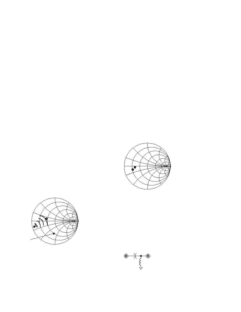
The input load pull parameter at 2 GHz is shown in
Figure 1 along with the optimum S11 conjugate match.
return loss will not be greater than 10 dB. For most ap
plications, a designer requires VSWR greater than 2:1,
hence limiting the input match close to S11*. Normally,
the input return loss of a single ended amplifier is not
critical as most basestation LNA and driver amplifiers
are in a balanced configuration with 90° (quadrature)
couplers.
Proceeding from the same premise, the output match
of this device becomes much simpler. As background
information, it is important to note that OIP3 is largely
dependant on the output match and that output return
loss is also required to be greater than 10 dB. So, Figure
2 shows how both good output return loss and good
linearity could be achieved simultaneously with the
same impedance point.
Of course, these points are valid only at 2 GHz, and
other frequencies will follow the same design rules but
will have different locations. Also, the location of these
points is largely due to the manufacturing process and
partly due to IC layout, but in either case beyond the
scope of this application note.
Figure 1. Input Match for ATF-521P8
GHz.
16
dB
5dB
9dB
3dB
S11*
Return
Loss
ΓS
Figure 2. Output Match
at 2 GHz.
S22*
ΓL
C1
RFin
RFout
L1
Figure 1. Input Match for ATF-521P8 at 2 GHz.
Thus, it should be obvious from the illustration above
that if this device is matched for maximum return
loss i.e. S11*, then OIP3 will be sacrificed. Conversely,
if ATF521P8 is matched for maximum linearity, then
Figure 2. Output Match at 2 GHz.
Once a designer has chosen the proper input and
output impedance points, the next step is to choose the
correct topology to accomplish this match. For example
to perform the above output impedance transformation
from 50 to the given load parameter of 0.53∠176°,
two possible solutions exist. The first potential match
is a high pass configuration accomplished by a shunt
inductor and a series capacitor shown in Figure 3 along
with its frequency response in Figure 4.
Figure 3. High Pass Circuit Topology.
相關(guān)PDF資料 |
PDF描述 |
|---|---|
| ATF-521P8-TR1 | L BAND, Si, N-CHANNEL, RF SMALL SIGNAL, HEMFET, MO-229 |
| ATF-521P8-BLK | L BAND, Si, N-CHANNEL, RF SMALL SIGNAL, HEMFET, MO-229 |
| ATF-53189-TR1 | C BAND, Si, N-CHANNEL, RF SMALL SIGNAL, HEMFET |
| ATF-53189-BLK | C BAND, Si, N-CHANNEL, RF SMALL SIGNAL, HEMFET |
| ATF-531P8-BLK | C BAND, Si, N-CHANNEL, RF SMALL SIGNAL, HEMFET, MO-229 |
相關(guān)代理商/技術(shù)參數(shù) |
參數(shù)描述 |
|---|---|
| ATF524S16M | 制造商:n/a 功能描述:Inverter Semiconductor |
| ATF-53189 | 制造商:AGILENT 制造商全稱:AGILENT 功能描述:Enhancement Mode Pseudomorphic HEMT in SOT 89 Package |
| ATF-53189-BLK | 功能描述:射頻GaAs晶體管 Transistor GaAs High Linearity RoHS:否 制造商:TriQuint Semiconductor 技術(shù)類型:pHEMT 頻率:500 MHz to 3 GHz 增益:10 dB 噪聲系數(shù): 正向跨導(dǎo) gFS(最大值/最小值):4 S 漏源電壓 VDS: 閘/源擊穿電壓:- 8 V 漏極連續(xù)電流:3 A 最大工作溫度:+ 150 C 功率耗散:10 W 安裝風(fēng)格: 封裝 / 箱體: |
| ATF-53189-TR1 | 功能描述:射頻GaAs晶體管 Transistor GaAs High Linearity RoHS:否 制造商:TriQuint Semiconductor 技術(shù)類型:pHEMT 頻率:500 MHz to 3 GHz 增益:10 dB 噪聲系數(shù): 正向跨導(dǎo) gFS(最大值/最小值):4 S 漏源電壓 VDS: 閘/源擊穿電壓:- 8 V 漏極連續(xù)電流:3 A 最大工作溫度:+ 150 C 功率耗散:10 W 安裝風(fēng)格: 封裝 / 箱體: |
| ATF-53189-TR2 | 功能描述:射頻GaAs晶體管 Transistor GaAs Hi gh Linearity RoHS:否 制造商:TriQuint Semiconductor 技術(shù)類型:pHEMT 頻率:500 MHz to 3 GHz 增益:10 dB 噪聲系數(shù): 正向跨導(dǎo) gFS(最大值/最小值):4 S 漏源電壓 VDS: 閘/源擊穿電壓:- 8 V 漏極連續(xù)電流:3 A 最大工作溫度:+ 150 C 功率耗散:10 W 安裝風(fēng)格: 封裝 / 箱體: |
發(fā)布緊急采購(gòu),3分鐘左右您將得到回復(fù)。