- 您現(xiàn)在的位置:買賣IC網(wǎng) > PDF目錄42903 > ATF-521P8-TR1 L BAND, Si, N-CHANNEL, RF SMALL SIGNAL, HEMFET, MO-229 PDF資料下載
參數(shù)資料
| 型號: | ATF-521P8-TR1 |
| 元件分類: | 小信號晶體管 |
| 英文描述: | L BAND, Si, N-CHANNEL, RF SMALL SIGNAL, HEMFET, MO-229 |
| 封裝: | 2 x 2 MM, 0.75 MM HEIGHT,LEAD FREE, PLASTIC,LPCC-8 |
| 文件頁數(shù): | 7/23頁 |
| 文件大小: | 319K |
| 代理商: | ATF-521P8-TR1 |
15
Figure 7 displays the input and output matching
selected for ATF521P8. In this example the input and
output match both essentially function as high pass
filters, but the high frequency gain of the device rolls off
precipitously giving a narrow band frequency response,
yet still wide enough to accommodate a CDMA or
WCDMA transmit band. For more information on RF
matching techniques refer to MGA53543 application
note.
Passive Bias[1]
Once the RF matching has been established, the next
step is to DC bias the device. A passive biasing example
is shown in Figure 8. In this example the voltage drop
across resistor R3 sets the drain current (Id) and is calcu
lated by the following equation:
R3 = V
dd – Vds
(1)
p
I
ds + Ibb
where,
V
dd is the power supply voltage;
V
ds is the device drain to source voltage;
I
ds is the device drain to source current;
I
bb for DC stability is 10X the typical gate current;
A voltage divider network with R1 and R2 establishes
the typical gate bias voltage (Vg).
R1 = V
g
(2)
p
I
bb
R2 = (Vdd – Vg) x R1
(3)
V
g
Often the series resistor, R4, is added to enhance the
low frequency stability. The complete passive bias
example may be found in reference [1].
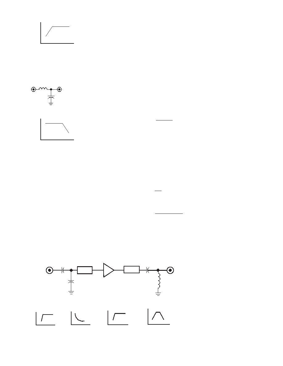
Figure 4. High Pass Frequency Response.
The second solution is a low pass configuration with a
shunt capacitor and a series inductor shown in Figure 5
and 6.
Figure 7. Input and Output Match for ATF-521P8 at 2 GHz.
Amp
Frequency
L1
RFin
RFout
C1
Amp
Frequency
+
=
Input Match
Amp
Frequency
Amp
ATF-521P8
Frequency
Amp
Output Match
Total Response
Amp
Frequency
Zo
52
C2
C1
C3
L1
RFout
RFin
Figure 5. Low Pass Circuit Topology.
Figure 6. Low Pass Frequency Response.
The actual values of these components may be calcu
lated by hand on a Smith Chart or more accurately done
on simulation software such as ADS. There are some
advantages and disadvantages of choosing a high pass
versus a low pass. For instance, a high pass circuit
cuts off low frequency gain, which narrows the usable
bandwidth of the amplifier, but consequently helps
avoid potential low frequency instability problems.
A low pass match offers a much broader frequency
response, but it has two major disadvantages. First it has
the potential for low frequency instability, and second it
creates the need for an extra DC blocking capacitor on
the input in order to isolate the device gate from the
preceding stages.
相關PDF資料 |
PDF描述 |
|---|---|
| ATF-521P8-BLK | L BAND, Si, N-CHANNEL, RF SMALL SIGNAL, HEMFET, MO-229 |
| ATF-53189-TR1 | C BAND, Si, N-CHANNEL, RF SMALL SIGNAL, HEMFET |
| ATF-53189-BLK | C BAND, Si, N-CHANNEL, RF SMALL SIGNAL, HEMFET |
| ATF-531P8-BLK | C BAND, Si, N-CHANNEL, RF SMALL SIGNAL, HEMFET, MO-229 |
| ATF-531P8-TR1G | C BAND, Si, N-CHANNEL, RF SMALL SIGNAL, HEMFET, MO-229 |
相關代理商/技術參數(shù) |
參數(shù)描述 |
|---|---|
| ATF-521P8-TR2 | 功能描述:射頻GaAs晶體管 Transistor GaAs High Linearity RoHS:否 制造商:TriQuint Semiconductor 技術類型:pHEMT 頻率:500 MHz to 3 GHz 增益:10 dB 噪聲系數(shù): 正向跨導 gFS(最大值/最小值):4 S 漏源電壓 VDS: 閘/源擊穿電壓:- 8 V 漏極連續(xù)電流:3 A 最大工作溫度:+ 150 C 功率耗散:10 W 安裝風格: 封裝 / 箱體: |
| ATF524S16M | 制造商:n/a 功能描述:Inverter Semiconductor |
| ATF-53189 | 制造商:AGILENT 制造商全稱:AGILENT 功能描述:Enhancement Mode Pseudomorphic HEMT in SOT 89 Package |
| ATF-53189-BLK | 功能描述:射頻GaAs晶體管 Transistor GaAs High Linearity RoHS:否 制造商:TriQuint Semiconductor 技術類型:pHEMT 頻率:500 MHz to 3 GHz 增益:10 dB 噪聲系數(shù): 正向跨導 gFS(最大值/最小值):4 S 漏源電壓 VDS: 閘/源擊穿電壓:- 8 V 漏極連續(xù)電流:3 A 最大工作溫度:+ 150 C 功率耗散:10 W 安裝風格: 封裝 / 箱體: |
| ATF-53189-TR1 | 功能描述:射頻GaAs晶體管 Transistor GaAs High Linearity RoHS:否 制造商:TriQuint Semiconductor 技術類型:pHEMT 頻率:500 MHz to 3 GHz 增益:10 dB 噪聲系數(shù): 正向跨導 gFS(最大值/最小值):4 S 漏源電壓 VDS: 閘/源擊穿電壓:- 8 V 漏極連續(xù)電流:3 A 最大工作溫度:+ 150 C 功率耗散:10 W 安裝風格: 封裝 / 箱體: |
發(fā)布緊急采購,3分鐘左右您將得到回復。