- 您現(xiàn)在的位置:買賣IC網(wǎng) > PDF目錄298831 > AS7C25512PFS32A-225BC (ALLIANCE SEMICONDUCTOR CORP) 512K X 32 STANDARD SRAM, 6.9 ns, PBGA165 PDF資料下載
參數(shù)資料
| 型號: | AS7C25512PFS32A-225BC |
| 廠商: | ALLIANCE SEMICONDUCTOR CORP |
| 元件分類: | SRAM |
| 英文描述: | 512K X 32 STANDARD SRAM, 6.9 ns, PBGA165 |
| 封裝: | BGA-165 |
| 文件頁數(shù): | 16/21頁 |
| 文件大小: | 458K |
| 代理商: | AS7C25512PFS32A-225BC |
AS7C25512PFS32A
AS7C25512PFS36A
12/2/02, v. 0.9.1
Alliance Semiconductor
4 of 21
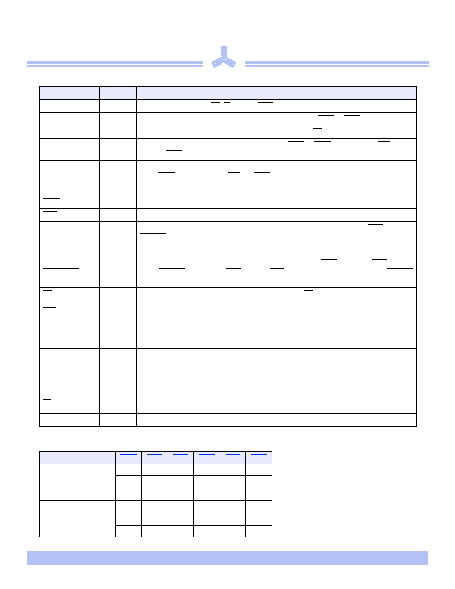
Signal descriptions
Write enable truth table (per byte)
.H\ X = don’t care, L = low, H = high, n = a, b, c, d; BWE, BWn = internal write signal.
Pin
I/O Properties Description
CLK
I
CLOCK
Clock. All inputs except OE, FT, ZZ, and LBO are synchronous to this clock.
A0–A19
I
SYNC
Address. Sampled when all chip enables are active and when ADSC or ADSP are asserted.
DQ[a,b,c,d] I/O
SYNC
Data. Driven as output when the chip is enabled and when OE is active.
CE0
ISYNC
Master chip enable. Sampled on clock edges when ADSP or ADSC is active. When CE0 is
inactive, ADSP is blocked. Refer to the “Synchronous truth table” for more information.
CE1, CE2
ISYNC
Synchronous chip enables, active high, and active low, respectively. Sampled on clock edges
when ADSC is active or when CE0 and ADSP are active.
ADSP
I
SYNC
Address strobe processor. Asserted low to load a new address or to enter standby mode.
ADSC
I
SYNC
Address strobe controller. Asserted low to load a new address or to enter standby mode.
ADV
I
SYNC
Advance. Asserted low to continue burst read/write.
GWE
ISYNC
Global write enable. Asserted low to write all 32/36 and 18 bits. When high, BWE and
BW[a:d] control write enable.
BWE
I
SYNC
Byte write enable. Asserted low with GWE high to enable effect of BW[a:d] inputs.
BW[a,b,c,d]
ISYNC
Write enables. Used to control write of individual bytes when GWE is high and BWE is low. If
any of BW[a:d] is active with GWE high and BWE low, the cycle is a write cycle. If all BW[a:d]
are inactive, the cycle is a read cycle.
OE
I
ASYNC
Asynchronous output enable. I/O pins are driven when OE is active and chip is in read mode.
LBO
ISTATIC
Count mode. When driven high, count sequence follows Intel XOR convention. When driven
low, count sequence follows linear convention. This signal is internally pulled high.
TDO
O
SYNC
Serial data-out to the JTAG circuit. Delivers data on the negative edge of TCK (BGA only).
TDI
I
SYNC
Serial data-in to the JTAG circuit. Sampled on the rising edge of TCK (BGA only).
TMS
I
SYNC
This pin controls the Test Access Port state machine. Sampled on the rising edge of TCK (BGA
only).
TCK
I
Test Clock
Test Clock. All inputs are sampled on the rising edge of TCK. All outputs are driven from the
falling edge of TCK.
FT
ISTATIC
Flow-through mode.When low, enables single register flow-through mode. Connect to VDD if
unused or for pipelined operation.
ZZ
I
ASYNC
Snooze. Places device in low power mode; data is retained. Connect to GND if unused.
Function
GWE
BWE
BWa
BWb
BWc
BWd
Write All Bytes
L
X
XXX
X
H
LLL
LL
Write Byte a
H
L
H
Write Byte c and d
H
L
H
L
Read
H
XXX
X
H
L
HH
相關(guān)PDF資料 |
PDF描述 |
|---|---|
| AS7C256A-10TCN | IC,AS7C256A-10TCN,TSOP-28 ASY SRAM,10NS,32K X 8,5V |
| AS7C31024-15PC | 128K X 8 STANDARD SRAM, 15 ns, PDIP32 |
| AS7C31024B-12TCN | IC,AS7C31024B-12TCN,TSOP-32 I, SRAM,12NS,128K X 8,3.3V |
| AS7C31026B-12TCN | IC,AS7C31026B-12TCN,TSOP-32 I, SRAM,12NS,64K X 16,3.3V |
| AS7C331MNTD32A-167TQCN | 1M X 32 ZBT SRAM, 7.5 ns, PQFP100 |
相關(guān)代理商/技術(shù)參數(shù) |
參數(shù)描述 |
|---|---|
| AS7C25512PFS36A-133TQC | 制造商:ALSC 制造商全稱:Alliance Semiconductor Corporation 功能描述:2.5V 512K x 32/36 pipelined burst synchronous SRAM |
| AS7C25512PFS36A-133TQCN | 制造商:ALSC 制造商全稱:Alliance Semiconductor Corporation 功能描述:2.5V 512K x 32/36 pipelined burst synchronous SRAM |
| AS7C25512PFS36A-133TQI | 制造商:ALSC 制造商全稱:Alliance Semiconductor Corporation 功能描述:2.5V 512K x 32/36 pipelined burst synchronous SRAM |
| AS7C25512PFS36A-133TQIN | 制造商:ALSC 制造商全稱:Alliance Semiconductor Corporation 功能描述:2.5V 512K x 32/36 pipelined burst synchronous SRAM |
| AS7C25512PFS36A-166TQC | 制造商:ALSC 制造商全稱:Alliance Semiconductor Corporation 功能描述:2.5V 512K x 32/36 pipelined burst synchronous SRAM |
發(fā)布緊急采購,3分鐘左右您將得到回復(fù)。