- 您現(xiàn)在的位置:買賣IC網(wǎng) > PDF目錄366550 > AM79C940VCW (ADVANCED MICRO DEVICES INC) Media Access Controller for Ethernet (MACE) PDF資料下載
參數(shù)資料
| 型號: | AM79C940VCW |
| 廠商: | ADVANCED MICRO DEVICES INC |
| 元件分類: | 微控制器/微處理器 |
| 英文描述: | Media Access Controller for Ethernet (MACE) |
| 中文描述: | 4 CHANNEL(S), 10M bps, LOCAL AREA NETWORK CONTROLLER, PQFP80 |
| 封裝: | TQFP-80 |
| 文件頁數(shù): | 22/122頁 |
| 文件大?。?/td> | 914K |
| 代理商: | AM79C940VCW |
第1頁第2頁第3頁第4頁第5頁第6頁第7頁第8頁第9頁第10頁第11頁第12頁第13頁第14頁第15頁第16頁第17頁第18頁第19頁第20頁第21頁當前第22頁第23頁第24頁第25頁第26頁第27頁第28頁第29頁第30頁第31頁第32頁第33頁第34頁第35頁第36頁第37頁第38頁第39頁第40頁第41頁第42頁第43頁第44頁第45頁第46頁第47頁第48頁第49頁第50頁第51頁第52頁第53頁第54頁第55頁第56頁第57頁第58頁第59頁第60頁第61頁第62頁第63頁第64頁第65頁第66頁第67頁第68頁第69頁第70頁第71頁第72頁第73頁第74頁第75頁第76頁第77頁第78頁第79頁第80頁第81頁第82頁第83頁第84頁第85頁第86頁第87頁第88頁第89頁第90頁第91頁第92頁第93頁第94頁第95頁第96頁第97頁第98頁第99頁第100頁第101頁第102頁第103頁第104頁第105頁第106頁第107頁第108頁第109頁第110頁第111頁第112頁第113頁第114頁第115頁第116頁第117頁第118頁第119頁第120頁第121頁第122頁
AMD
22
Am79C940
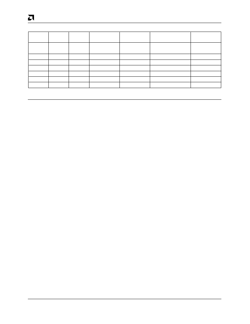
DXCVR Configuration—Normal Operation
SLEEP
Pin
ASEL
Bit
LNKST
Pin
PORTSEL
[1–0] Bits
ENPLSIO
Bit
Interface
Description
Pin
Function
1
X
X
XX
X
SIA Test Mode
High
Impedance
LOW
HIGH
HIGH
LOW
LOW
HIGH
1
1
1
1
1
1
0
0
0
0
1
1
X
X
X
X
00
01
10
11
0X
0X
X
X
X
X
X
X
AUI
10BASE-T
DAI Port
GPSI
AUI
10BASE-T
HIGH
LOW
Note:
RWAKE and ASEL are located in the PHY Configuration Control register (REG ADDR 15). PORTSEL [1–0] and
ENPLSIO are located in the PLS Configuration Control register (REG ADDR 14).
10BASE-T Interface
TXD+, TXD–
Transmit Data (Output)
10BASE-T port differential drivers.
TXP+, TXP–
Transmit Pre-Distortion (Output)
Transmit wave form differential driver for pre-distortion.
RXD+, RXD–
Receive Data (Input)
10BASE-T port differential receiver. These pins should
be externally terminated to reduce power consumption if
the 10BASE-T interface is not used.
LNKST
Link Status (OutputOpen Drain)
This pin is driven LOW if the link is identified as func-
tional. If the link is determined to be nonfunctional, due
to missing idle link pulses or data packets, then this pin
is not driven (requires external pull-up). In the LOW out-
put state, the pin is capable of sinking a maximum of
12 mA and can be used to drive an LED.
This feature can be disabled by setting the Disable Link
Test (DLNKTST) bit in the PHY Configuration Control
register. In this case the internal Link Test Receive func-
tion is disabled, the
LNKST
pin will be driven LOW, and
the Transmit and Receive functions will remain active
regardless of arriving idle link pulses and data. The in-
ternal 10BASE-T MAU will continue to generate idle link
pulses irrespective of the status of the DLNKTST bit.
RXPOL
Receive Polarity (Output,Open Drain)
The twisted pair receiver is capable of detecting a re-
ceive signal with reversed polarity (wiring error). The
RXPOL
pin is normally in the LOW state, indicating cor-
rect polarity of the received signal. If the receiver detects
a received packet with reversed polarity, then this pin is
not driven (requires external pull–up) and the polarity of
subsequent packets are inverted. In the LOW output
state, this pin is capable of sinking a maximum of 12mA
and can be used to drive an LED.
The polarity correction feature can be disabled by set-
ting the Disable Auto Polarity Correction (DAPC) bit in
the PHY Configuration Control register. In this case, the
Receive Polarity correction circuit is disabled and the in-
ternal receive signal remains non-inverted, irrespective
of the received signal. Note that
RXPOL
will continue to
reflect the polarity detected by the receiver.
General Purpose Serial Interface (GPSI)
STDCLK
Serial Transmit Data Clock (Input/Output)
When either the AUI, 10BASE-T or DAI port is selected,
STDCLK is an output operating at one half the crystal or
XTAL1 frequency. STDCLK is the encoding clock for
Manchester data transferred to the output of either the
AUI DO
±
pair, the 10BASE-T TXD
±
/TXP
±
pairs, or the
DAI port TXDAT
±
pair. When using the GPSI port,
STDCLK is an input at the network data rate, provided
by the external Manchester encode/decoder, to strobe
out the NRZ data presented on the TXDAT+ output.
相關PDF資料 |
PDF描述 |
|---|---|
| AM79C940 | Media Access Controller for Ethernet (MACE) |
| AM79C940JCW | Media Access Controller for Ethernet (MACE) |
| AM79C940KCW | Media Access Controller for Ethernet (MACE) |
| AM79C960 | PCnetTM-ISA Single-Chip Ethernet Controller |
| AM79C960KC | PCnetTM-ISA Single-Chip Ethernet Controller |
相關代理商/技術(shù)參數(shù) |
參數(shù)描述 |
|---|---|
| AM79C940VI | 制造商:未知廠家 制造商全稱:未知廠家 功能描述:LAN Node Controller |
| AM79C940VI/W | 制造商:未知廠家 制造商全稱:未知廠家 功能描述:LAN Node Controller |
| AM79C945 | 制造商:未知廠家 制造商全稱:未知廠家 功能描述: |
| AM79C945-16 | 制造商:未知廠家 制造商全稱:未知廠家 功能描述: |
| AM79C945-16JC | 制造商:未知廠家 制造商全稱:未知廠家 功能描述:LAN Node Controller |
發(fā)布緊急采購,3分鐘左右您將得到回復。