- 您現(xiàn)在的位置:買賣IC網(wǎng) > PDF目錄362278 > AM486DX Am486DX - Am486DX Block Diagram PDF資料下載
參數(shù)資料
| 型號: | AM486DX |
| 英文描述: | Am486DX - Am486DX Block Diagram |
| 中文描述: | Am486DX - Am486DX框圖 |
| 文件頁數(shù): | 24/52頁 |
| 文件大?。?/td> | 1242K |
| 代理商: | AM486DX |
第1頁第2頁第3頁第4頁第5頁第6頁第7頁第8頁第9頁第10頁第11頁第12頁第13頁第14頁第15頁第16頁第17頁第18頁第19頁第20頁第21頁第22頁第23頁當(dāng)前第24頁第25頁第26頁第27頁第28頁第29頁第30頁第31頁第32頁第33頁第34頁第35頁第36頁第37頁第38頁第39頁第40頁第41頁第42頁第43頁第44頁第45頁第46頁第47頁第48頁第49頁第50頁第51頁第52頁
24
Am486DE2 Microprocessor
(including emptying the write buffers), and before the
first access to SMRAM when the CPU saves (writes) its
state (or context) to SMRAM. SMIACT remains active
until the last access to SMRAM when the CPU restores
(reads) its state from SMRAM. The SMIACT signal does
not float in response to HOLD. The SMIACT signal is
used by the system logic to decode SMRAM. The num-
ber of clocks required to complete the SMM state save
and restore is dependent on system memory perfor-
mance. The values shown in Figure 7 assume 0 wait-
state memory writes (two clock cycles), 2 – 1 – 1 – 1
burst read cycles, and 0 wait-state non-burst reads (two
clock cycles). Additionally, it is assumed that the data
read during the SMM-state-restore sequence is not
cacheable. The minimum time required to enter an
SMSAVE SMI handler routine for the CPU (from the
completion of the interrupted instruction) is given by:
Latency to start of SMl handler = A + B + C = 161 clocks
and the minimum time required to return to the interrupt-
ed application (following the final SMM instruction be-
fore RSM) is given by:
Latency to continue application = E + F + G = 258 clocks
SMRAM
The CPU uses the SMRAM space for state-save and
state-restore operations during an SMI. The SMI han-
dler, which also resides in SMRAM, uses the SMRAM
space to store code, data, and stacks. In addition, the
SMI handler can use the SMRAM for system manage-
ment information such as the system configuration, con-
figuration of a powered-down device, and system
designer-specific information.
Note:
Access to SMRAM is through the CPU internal
cache. To ensure cache consistency and correct oper-
ation, always assert the FLUSH pin in the same clock
as SMI for systems using overlaid SMRAM.
The CPU asserts SMIACT to indicate to the memory
controller that it is operating in System Management
Mode. The system logic should ensure that only the CPU
and SMI handler have access to this area. Alternate bus
masters or DMA devices trying to access the SMRAM
space when SMIACT is active should be directed to sys-
tem RAM in the respective area. The system logic is
minimally required to decode the physical memory ad-
dress range from 38000h–3FFFFh as SMRAM area.
The CPU saves its state to the state-save area from
3FFFFh downward to 3FE00h. After saving its state, the
CPU jumps to the address location 38000h to begin ex-
ecuting the SMI handler. The system logic can choose
to decode a larger area of SMRAM as needed. The size
of this SMRAM can be between 32 Kbyte and
4 Gbyte.The system logic should provide a manual
method for switching the SMRAM into system memory
space when the CPU is not in SMM. This enables ini-
tialization of the SMRAM space (i.e., loading SMI han-
dler) before executing the SMI handler during SMM (see
Figure 8).
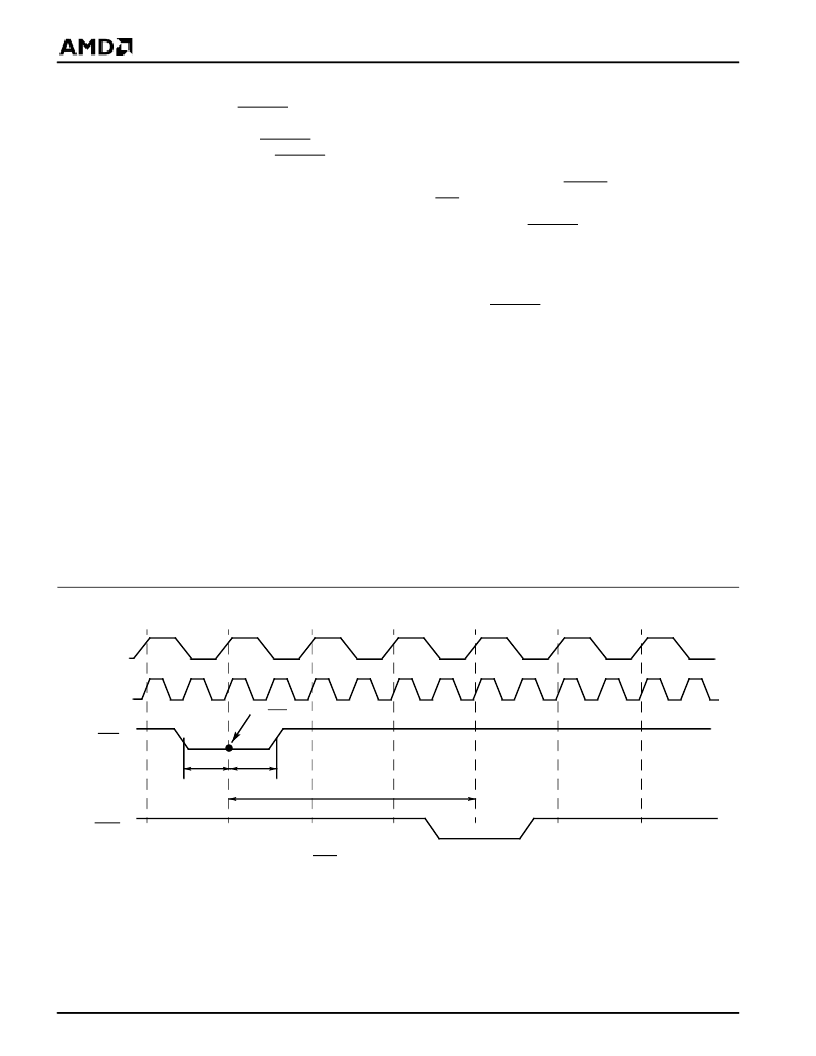
Figure 6. SMI Timing for Servicing an I/O Trap
tsu
thd
SMI Sampled
CLK
CLK2
SMI
RDY
相關(guān)PDF資料 |
PDF描述 |
|---|---|
| AM486DXPGA | Am486DX PGA - Am486DX PGA Package Temperature Comparisons |
| AM486DXSQFP | 70NS, PLCC, IND TEMP(EEPROM) |
| AM486 | Am486 Microprocessor Software User's Manual? 4.40MB (PDF) |
| AM49DL3208G | Am49DL3208G - Stacked Multi-Chip Package (MCP) Flash Memory and pSRAM |
| AM49DL320BG | Am49DL320BG - Stacked Multi-Chip Package (MCP) Flash Memory and SRAM |
相關(guān)代理商/技術(shù)參數(shù) |
參數(shù)描述 |
|---|---|
| AM486DX/DX2 | 制造商:未知廠家 制造商全稱:未知廠家 功能描述:Am486DX/DX2 Hardware Reference Manual |
| AM486DX2 | 制造商:AMD 制造商全稱:Advanced Micro Devices 功能描述:Am5X86⑩ Microprocessor Family |
| AM486DX2-66V16BGC | 制造商:Advanced Micro Devices 功能描述:MPU AM486 RISC 32-Bit 0.35um 66MHz 5V 168-Pin PGA |
| AM486DX2-66V16BGI | 制造商:Advanced Micro Devices 功能描述:MPU AM486 RISC 32-Bit 0.35um 66MHz 5V 168-Pin PGA |
| AM486DX2-66V16BHI | 制造商:Advanced Micro Devices 功能描述:MPU AM486 RISC 32-Bit 0.35um 66MHz 5V 208-Pin SQFP |
發(fā)布緊急采購,3分鐘左右您將得到回復(fù)。