- 您現(xiàn)在的位置:買賣IC網(wǎng) > PDF目錄362278 > AM486DE2 Am486DE2 Microprocessor Data Sheet PDF資料下載
參數(shù)資料
| 型號: | AM486DE2 |
| 英文描述: | Am486DE2 Microprocessor Data Sheet |
| 中文描述: | Am486DE2微處理器數(shù)據(jù)表 |
| 文件頁數(shù): | 19/52頁 |
| 文件大小: | 1242K |
| 代理商: | AM486DE2 |
第1頁第2頁第3頁第4頁第5頁第6頁第7頁第8頁第9頁第10頁第11頁第12頁第13頁第14頁第15頁第16頁第17頁第18頁當前第19頁第20頁第21頁第22頁第23頁第24頁第25頁第26頁第27頁第28頁第29頁第30頁第31頁第32頁第33頁第34頁第35頁第36頁第37頁第38頁第39頁第40頁第41頁第42頁第43頁第44頁第45頁第46頁第47頁第48頁第49頁第50頁第51頁第52頁
Am486DE2 Microprocessor
19
Stop Grant Bus Cycle
The processor drives a special Stop Grant bus cycle to
the bus after recognizing the STPCLK interrupt. This bus
cycle is the same as the HALT cycle used by a standard
Am486 microprocessor, with the exception that the Stop
Grant bus cycle drives the value 0000 0010h on the
address pins.
I
M/lO = 0
I
D/C = 0
I
W/R =1
I
Address Bus = 0000 0010h (A
4
= 1)
I
BE3–BE0 = 1011
I
Data bus = undefined
The system hardware must acknowledge this cycle by
returning RDY or BRDY, or the processor will not enter
the Stop Grant state (see Figure 1). The latency be-
tween a STPCLK request and the Stop Grant bus cycle
depends on the current instruction, the amount of data
in the CPU write buffers, and the system memory per-
formance.
Pin State During Stop Grant
Table 2 shows the pin states during Stop Grant bus
states. During the Stop Grant state, most output and in-
put/output signals of the microprocessor maintain the
level they held when entering the Stop Grant state. The
data and data parity signals are three-stated. In response
to HOLD being driven active during the Stop Grant state
(when the CLK input is running), the CPU generates
HLDA and three-states all output and input/output sig-
nals that are three-stated during the HOLD/HLDA state.
After HOLD is deasserted, all signals return to the same
state they were before the HOLD/HLDA sequence.
To achieve the lowest possible power consumption during
the Stop Grant state, the system designer must ensure the
input signals with pull-up resistors are not driven Low, and
the input signals with pull-down resistors are not driven High.
All inputs except data bus pins must be driven to the
power supply rails to ensure the lowest possible current
consumption during Stop Grant or Stop Clock modes.
For compatibility, data pins must be driven Low to
achieve the lowest possible power consumption.
Table 2. Pin State During Stop Grant Bus State
Signal
Type
State
A3–A2
O
Previous State
A31–A4
I/O
Previous State
D31–D0
I/O
Floated
BE3–BE0
O
Previous State
DP3–DP0
I/O
Floated
W/R, D/C, M/IO, CACHE
O
Previous State
ADS
O
Inactive
LOCK, PLOCK
O
Inactive
BREQ
O
Previous State
HLDA
O
As per HOLD
BLAST
O
Previous State
FERR
O
Previous State
PCHK
O
Previous State
SMIACT
O
Previous State
HITM
O
Previous State
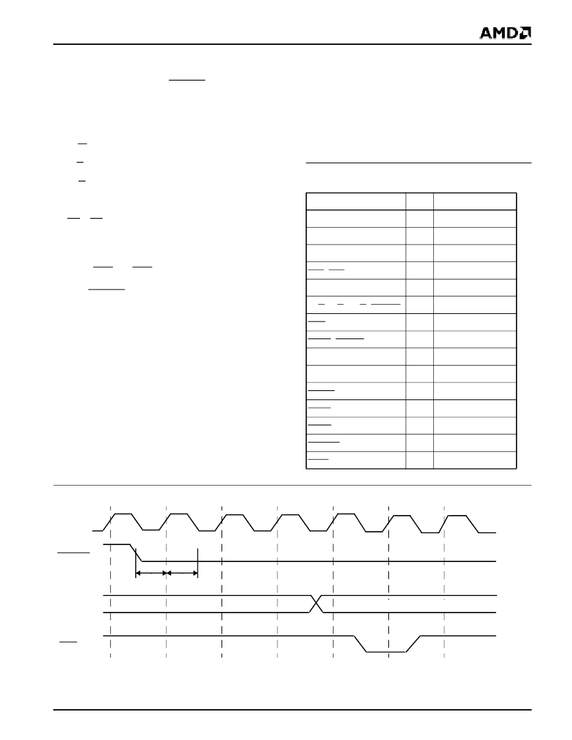
Figure 1. Entering Stop Grant State
t
20
t
21
RDY
ADDR
STPCLK
CLK
Stop Grant Bus cycle
相關(guān)PDF資料 |
PDF描述 |
|---|---|
| AM486DX | Am486DX - Am486DX Block Diagram |
| AM486DXPGA | Am486DX PGA - Am486DX PGA Package Temperature Comparisons |
| AM486DXSQFP | 70NS, PLCC, IND TEMP(EEPROM) |
| AM486 | Am486 Microprocessor Software User's Manual? 4.40MB (PDF) |
| AM49DL3208G | Am49DL3208G - Stacked Multi-Chip Package (MCP) Flash Memory and pSRAM |
相關(guān)代理商/技術(shù)參數(shù) |
參數(shù)描述 |
|---|---|
| AM486DE2-66V8TGC | 制造商:AMD 制造商全稱:Advanced Micro Devices 功能描述:8-Kbyte Write-Through Embedded Microprocessor |
| AM486DE2-66V8THC | 制造商:Advanced Micro Devices 功能描述:Microprocessor, 32 Bit, 208 Pin, Plastic, QFP |
| AM486DX | 制造商:未知廠家 制造商全稱:未知廠家 功能描述:Am486DX - Am486DX Block Diagram |
| AM486DX/DX2 | 制造商:未知廠家 制造商全稱:未知廠家 功能描述:Am486DX/DX2 Hardware Reference Manual |
| AM486DX2 | 制造商:AMD 制造商全稱:Advanced Micro Devices 功能描述:Am5X86⑩ Microprocessor Family |
發(fā)布緊急采購,3分鐘左右您將得到回復(fù)。