- 您現(xiàn)在的位置:買賣IC網(wǎng) > PDF目錄352474 > AM42BDS640AGBD9IT (SPANSION LLC) Stacked Multi-Chip Package (MCP) Flash Memory and SRAM PDF資料下載
參數(shù)資料
| 型號(hào): | AM42BDS640AGBD9IT |
| 廠商: | SPANSION LLC |
| 元件分類: | 存儲(chǔ)器 |
| 英文描述: | Stacked Multi-Chip Package (MCP) Flash Memory and SRAM |
| 中文描述: | SPECIALTY MEMORY CIRCUIT, PBGA93 |
| 封裝: | 8 X 11.60 MM, FBGA-93 |
| 文件頁(yè)數(shù): | 66/72頁(yè) |
| 文件大小: | 1060K |
| 代理商: | AM42BDS640AGBD9IT |
第1頁(yè)第2頁(yè)第3頁(yè)第4頁(yè)第5頁(yè)第6頁(yè)第7頁(yè)第8頁(yè)第9頁(yè)第10頁(yè)第11頁(yè)第12頁(yè)第13頁(yè)第14頁(yè)第15頁(yè)第16頁(yè)第17頁(yè)第18頁(yè)第19頁(yè)第20頁(yè)第21頁(yè)第22頁(yè)第23頁(yè)第24頁(yè)第25頁(yè)第26頁(yè)第27頁(yè)第28頁(yè)第29頁(yè)第30頁(yè)第31頁(yè)第32頁(yè)第33頁(yè)第34頁(yè)第35頁(yè)第36頁(yè)第37頁(yè)第38頁(yè)第39頁(yè)第40頁(yè)第41頁(yè)第42頁(yè)第43頁(yè)第44頁(yè)第45頁(yè)第46頁(yè)第47頁(yè)第48頁(yè)第49頁(yè)第50頁(yè)第51頁(yè)第52頁(yè)第53頁(yè)第54頁(yè)第55頁(yè)第56頁(yè)第57頁(yè)第58頁(yè)第59頁(yè)第60頁(yè)第61頁(yè)第62頁(yè)第63頁(yè)第64頁(yè)第65頁(yè)當(dāng)前第66頁(yè)第67頁(yè)第68頁(yè)第69頁(yè)第70頁(yè)第71頁(yè)第72頁(yè)
68
Am42BDS640AG
November 1, 2002
P R E L I M INARY
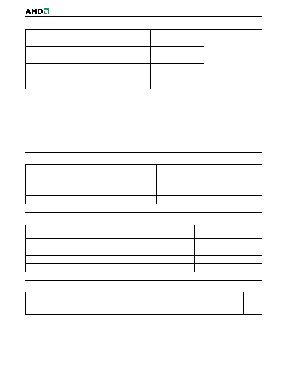
FLASH ERASE AND PROGRAMMING PERFORMANCE
Notes:
1. Typical program and erase times assume the following conditions: 25
°C, 2.0 V V
CC, 1,000,000 cycles. Additionally,
programming typicals assume checkerboard pattern.
2. Under worst case conditions of 90
°C, V
CC = 1.8 V, 1,000,000 cycles.
3. The typical chip programming time is considerably less than the maximum chip programming time listed, since most bytes
program faster than the maximum program times listed.
4. In the pre-programming step of the Embedded Erase algorithm, all bytes are programmed to 00h before erasure.
5. System-level overhead is the time required to execute the two- or four-bus-cycle sequence for the program command. See Table
14 for further information on command definitions.
6. The device has a minimum erase and program cycle endurance of 1,000,000 cycles.
FLASH LATCHUP CHARACTERISTICS
Note: Includes all pins except V
CC. Test conditions: VCC = 3.0 V, one pin at a time.
PACKAGE PIN CAPACITANCE
Note:Test conditions T
A = 25°C, f = 1.0 MHz.
FLASH DATA RETENTION
Parameter
Typ (Note 1)
Max (Note 2)
Unit
Comments
Sector Erase Time (32 Kword or 8 Kword)
0.4
5
sec
Excludes 00h programming
prior to erasure (Note 4)
Chip Erase Time
54
sec
Word Program Time
11.5
210
s
Excludes system level
overhead (Note 5)
Accelerated Word Program Time
4
120
s
Chip Program Time (Note 3)
48
144
sec
Accelerated Chip Program Time
16
48
sec
Description
Min
Max
Input voltage with respect to VSS on all pins except I/O pins
(including OE#, and RESET#)
–1.0 V
12.5 V
Input voltage with respect to V
SS on all I/O pins
–1.0 V
V
CC + 1.0 V
V
CC Current
–100 mA
+100 mA
Parameter
Symbol
Description
Test Setup
Typ
Max
Unit
C
IN
Input Capacitance
V
IN = 0
11
14
pF
C
OUT
Output Capacitance
V
OUT = 0
12
16
pF
C
IN2
Control Pin Capacitance
V
IN = 0
14
16
pF
C
IN3
WP#/ACC Pin Capacitance
V
IN = 0
17
20
pF
Parameter Description
Test Conditions
Min
Unit
Minimum Pattern Data Retention Time
150
°C10
Years
125
°C20
Years
相關(guān)PDF資料 |
PDF描述 |
|---|---|
| AM29F017D-150FE | LM340/LM78XX Series 3-Terminal Positive Regulators; Package: TO-3; No of Pins: 2; Qty per Container: 50; Container: Tray |
| AM29F017D-150FI | LM340/LM78XX Series 3-Terminal Positive Regulators; Package: TO-3; No of Pins: 2; Qty per Container: 50; Container: Tray |
| AM29F017D-70E4C | LM340/LM78XX Series 3-Terminal Positive Regulators; Package: TO-3; No of Pins: 2; Qty per Container: 50; Container: Tray |
| AM29F017D-70E4E | LM140L/LM340L Series 3-Terminal Positive Regulators; Package: TO-39; No of Pins: 3; Qty per Container: 500; Container: Box |
| AM29F017D-70E4I | LM140L/LM340L Series 3-Terminal Positive Regulators; Package: TO-39; No of Pins: 3; Qty per Container: 500; Container: Box |
相關(guān)代理商/技術(shù)參數(shù) |
參數(shù)描述 |
|---|---|
| AM42BDS640AGTC8IS | 制造商:AMD 制造商全稱:Advanced Micro Devices 功能描述:64 Megabit (4 M x 16-Bit) CMOS 1.8 Volt-only, Simultaneous Operation, Burst Mode Flash Memory and 16 Mbit (1 M x 16-Bit) Static RAM |
| AM42BDS640AGTC8IT | 制造商:AMD 制造商全稱:Advanced Micro Devices 功能描述:64 Megabit (4 M x 16-Bit) CMOS 1.8 Volt-only, Simultaneous Operation, Burst Mode Flash Memory and 16 Mbit (1 M x 16-Bit) Static RAM |
| AM42BDS640AGTC9IS | 制造商:AMD 制造商全稱:Advanced Micro Devices 功能描述:64 Megabit (4 M x 16-Bit) CMOS 1.8 Volt-only, Simultaneous Operation, Burst Mode Flash Memory and 16 Mbit (1 M x 16-Bit) Static RAM |
| AM42BDS640AGTC9IT | 制造商:AMD 制造商全稱:Advanced Micro Devices 功能描述:64 Megabit (4 M x 16-Bit) CMOS 1.8 Volt-only, Simultaneous Operation, Burst Mode Flash Memory and 16 Mbit (1 M x 16-Bit) Static RAM |
| AM42BDS640AGTD8IS | 制造商:AMD 制造商全稱:Advanced Micro Devices 功能描述:64 Megabit (4 M x 16-Bit) CMOS 1.8 Volt-only, Simultaneous Operation, Burst Mode Flash Memory and 16 Mbit (1 M x 16-Bit) Static RAM |
發(fā)布緊急采購(gòu),3分鐘左右您將得到回復(fù)。