- 您現(xiàn)在的位置:買賣IC網(wǎng) > PDF目錄165354 > ADS1194CZXGT (TEXAS INSTRUMENTS INC) SPECIALTY ANALOG CIRCUIT, PBGA64 PDF資料下載
參數(shù)資料
| 型號: | ADS1194CZXGT |
| 廠商: | TEXAS INSTRUMENTS INC |
| 元件分類: | 模擬信號調(diào)理 |
| 英文描述: | SPECIALTY ANALOG CIRCUIT, PBGA64 |
| 封裝: | 8 X 8 MM, GREEN, PLASTIC, NFBGA-64 |
| 文件頁數(shù): | 33/76頁 |
| 文件大?。?/td> | 1193K |
| 代理商: | ADS1194CZXGT |
第1頁第2頁第3頁第4頁第5頁第6頁第7頁第8頁第9頁第10頁第11頁第12頁第13頁第14頁第15頁第16頁第17頁第18頁第19頁第20頁第21頁第22頁第23頁第24頁第25頁第26頁第27頁第28頁第29頁第30頁第31頁第32頁當(dāng)前第33頁第34頁第35頁第36頁第37頁第38頁第39頁第40頁第41頁第42頁第43頁第44頁第45頁第46頁第47頁第48頁第49頁第50頁第51頁第52頁第53頁第54頁第55頁第56頁第57頁第58頁第59頁第60頁第61頁第62頁第63頁第64頁第65頁第66頁第67頁第68頁第69頁第70頁第71頁第72頁第73頁第74頁第75頁第76頁
1
9
17
25
CS
(1)
SCLK
DIN
OPCODE1
OPCODE2
DOUT
REGDATA
REGDATA+1
1
9
17
25
CS
(1)
SCLK
DIN
OPCODE1
OPCODE2
REGDATA1
REGDATA2
DOUT
SBAS471B
– APRIL 2010 – REVISED APRIL 2011
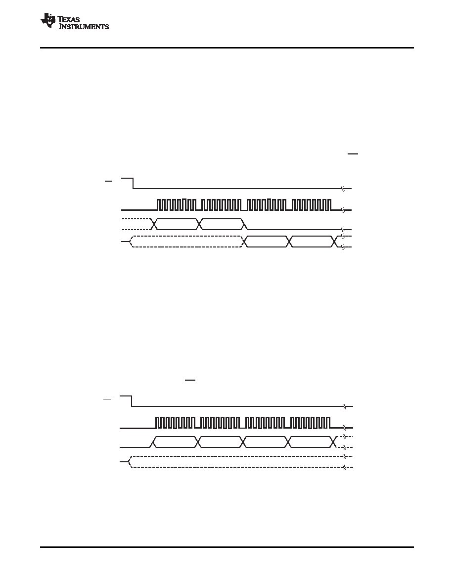
RREG: Read From Register
This opcode reads register data. The Register Read command is a two-byte opcode followed by the output of the
register data. The first byte contains the command opcode and the register address. The second byte of the
opcode specifies the number of registers to read
– 1.
First opcode byte: 0010 rrrr, where rrrr is the starting register address.
Second opcode byte: 000n nnnn, where n nnnn is the number of registers to read
– 1.
The 17th SCLK rising edge of the operation clocks out the MSB of the first register, as shown in Figure 40. When
the device is in read data continuous mode it is necessary to issue a SDATAC command before RREG
command can be issued. RREG command can be issued any time. However, because this command is a
multi-byte command, there are restrictions on the SCLK rate depending on the way the SCLKs are issued. See
the Serial Clock (SCLK) subsection of the SPI Interface section for more details. Note that CS must be low for
the entire command.
Figure 40. RREG Command Example: Read Two Registers Starting from Register 00h (ID Register)
(OPCODE 1 = 0010 0000, OPCODE 2 = 0000 0001)
WREG: Write to Register
This opcode writes register data. The Register Write command is a two-byte opcode followed by the input of the
register data. The first byte contains the command opcode and the register address.
The second byte of the opcode specifies the number of registers to write
– 1.
First opcode byte: 0100 rrrr, where rrrr is the starting register address.
Second opcode byte: 000n nnnn, where n nnnn is the number of registers to write
– 1.
After the opcode bytes, the register data follows (in MSB-first format), as shown in Figure 41. WREG command
can be issued any time. However, because this command is a multi-byte command, there are restrictions on the
SCLK rate depending on the way the SCLKs are issued. See the Serial Clock (SCLK) subsection of the SPI
Interface section for more details. Note that CS must be low for the entire command.
Figure 41. WREG Command Example: Write Two Registers Starting from 00h (ID Register)
(OPCODE 1 = 0100 0000, OPCODE 2 = 0000 0001)
Copyright
2010–2011, Texas Instruments Incorporated
39
相關(guān)PDF資料 |
PDF描述 |
|---|---|
| ADS1251 | "ResolutionPlus 24-Bit |
| ADS5102IPFBR | 1.8-V ANALOG SUPPLY, 10-BIT, 65/40 MSPS ANALOG-TO-DIGITAL CONVERTERS WITH INTERNAL REFERENCE |
| ADS5103 | "10 Bit |
| ADS5103CPFB | 1.8-V ANALOG SUPPLY, 10-BIT, 65/40 MSPS ANALOG-TO-DIGITAL CONVERTERS WITH INTERNAL REFERENCE |
| ADS5103CPFBR | 1.8-V ANALOG SUPPLY, 10-BIT, 65/40 MSPS ANALOG-TO-DIGITAL CONVERTERS WITH INTERNAL REFERENCE |
相關(guān)代理商/技術(shù)參數(shù) |
參數(shù)描述 |
|---|---|
| ADS1194IPAG | 制造商:TI 制造商全稱:Texas Instruments 功能描述:Low-Power 8-Channel 16-Bit Analog Front-End for Biopotential Measurements |
| ADS1194IPAGR | 制造商:TI 制造商全稱:Texas Instruments 功能描述:Low-Power 8-Channel 16-Bit Analog Front-End for Biopotential Measurements |
| ADS1196 | 制造商:TI 制造商全稱:Texas Instruments 功能描述:Low-Power, 8-Channel, 24-Bit Analog Front-End for Biopotential Measurements |
| ADS1196CPAG | 功能描述:模數(shù)轉(zhuǎn)換器 - ADC Low-Pwr6Ch16B Ana Front-End for ECG RoHS:否 制造商:Texas Instruments 通道數(shù)量:2 結(jié)構(gòu):Sigma-Delta 轉(zhuǎn)換速率:125 SPs to 8 KSPs 分辨率:24 bit 輸入類型:Differential 信噪比:107 dB 接口類型:SPI 工作電源電壓:1.7 V to 3.6 V, 2.7 V to 5.25 V 最大工作溫度:+ 85 C 安裝風(fēng)格:SMD/SMT 封裝 / 箱體:VQFN-32 |
| ADS1196CPAG | 制造商:Texas Instruments 功能描述:; Resolution (Bits):16bit; Sampling Rate 制造商:Texas Instruments 功能描述:IC, ADC, 6CH, 16BIT, 8KSPS, TQFP-64 |
發(fā)布緊急采購,3分鐘左右您將得到回復(fù)。