- 您現(xiàn)在的位置:買賣IC網(wǎng) > PDF目錄374016 > ADMCF341-EVALKIT (Analog Devices, Inc.) DashDSP⑩ 28-Lead Flash Mixed-Signal DSP with Enhanced Analog Front End PDF資料下載
參數(shù)資料
| 型號(hào): | ADMCF341-EVALKIT |
| 廠商: | Analog Devices, Inc. |
| 英文描述: | DashDSP⑩ 28-Lead Flash Mixed-Signal DSP with Enhanced Analog Front End |
| 中文描述: | DashDSP⑩28引腳閃存混合信號(hào)增強(qiáng)的DSP與模擬前端 |
| 文件頁數(shù): | 7/36頁 |
| 文件大小: | 1106K |
| 代理商: | ADMCF341-EVALKIT |
第1頁第2頁第3頁第4頁第5頁第6頁當(dāng)前第7頁第8頁第9頁第10頁第11頁第12頁第13頁第14頁第15頁第16頁第17頁第18頁第19頁第20頁第21頁第22頁第23頁第24頁第25頁第26頁第27頁第28頁第29頁第30頁第31頁第32頁第33頁第34頁第35頁第36頁
REV. 0
ADMCF341
–7–
GENERAL DESCRIPTION
The ADMCF341 is a low-cost, single-chip DSP-based control-
ler, suitable for permanent magnet synchronous motors, ac
induction motors, and brushless dc motors. The ADMCF341
integrates a 20 MHz, fixed-point DSP core with a complete set
of motor control and system peripherals that permits fast,
efficient development of motor controllers.
The DSP core of the ADMCF341 is completely code-compatible
with the ADSP-21xx DSP family and combines three computa-
tional units, data address generators, and a program sequencer.
The computational units are an ALU, a multiplier/accumulator
(MAC), and a barrel shifter. There are special instructions for
bit manipulation, multiplication ( squared), biased rounding,
and global interrupt masking. The system peripherals are the
power-on reset circuit (POR), the watchdog timer, and two
synchronous serial ports. The serial ports are configurable and
double buffered, with hardware support for UART, SCI, and
SPI port emulation. The ADMCF341 provides 512
program memory RAM, 4K
24-bit program memory ROM,
4K
24-bit program FLASH memory, and 512
memory RAM. The user code can be stored and executed from
the flash memory. The program and data memory RAM can be
used for dynamic data storage or can be loaded through the
serial port from an external device as in other ADMCxxx family
parts. The program memory ROM contains a monitor function
as well as useful routines for erasing, programming, and verifying
the flash memory.
The motor control peripherals of the ADMCF341 provide a
12-bit analog data acquisition system with six analog input
channels with three dedicated I
SENSE
inputs (combining internal
amplification, sampling, and overcurrent PWM shutdown
features) and an internal voltage reference. In addition, a three-
phase, 16-bit, center-based PWM generation unit can be used
24-bit
16-bit data
to produce high accuracy PWM signals with minimal processor
overhead. The ADMCF341 also contains two 16-bit auxiliary
PWM timer outputs and nine lines of digital I/O.
Because the ADMCF341 has a limited number of pins, functions
such as the auxiliary PWM timers and the serial communication
ports are multiplexed with the nine programmable digital input/
output (PIO) pins. The pin functions can be independently
selected to allow maximum flexibility for different applications.
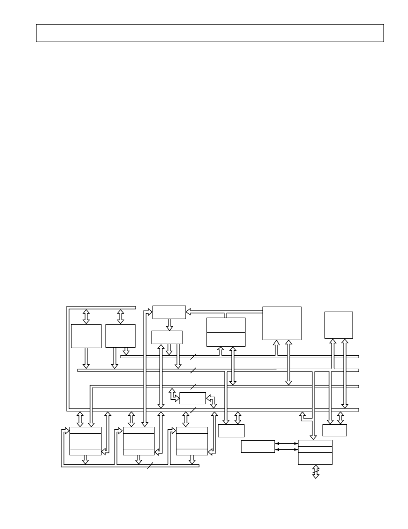
DSP CORE ARCHITECTURE OVERVIEW
Figure 3 is an overall block diagram of the DSP core of the
ADMCF341. The flexible architecture and comprehensive
instruction set allow the processor to perform multiple opera-
tions in parallel. In one processor cycle (50 ns with a 10 MHz
CLKIN) the DSP core can:
∑
∑
∑
∑
∑
This all takes place while the processor continues to:
∑
∑
∑
∑
∑
∑
Generate the next program address
Fetch the next instruction
Perform one or two data moves
Update one or two data address pointers
Perform a computational operation
Receive and transmit through the serial ports
Decrement the interval timer
Generate three-phase PWM waveforms for a power inverter
Generate two signals using the 16-bit auxiliary PWM timers
Acquire four analog signals
Decrement the watchdog timer
PM ROM
4K 24
PM RAM
512 24
BUS
EXCHANGE
COMPANDING
CIRCUITRY
DATA
ADDRESS
GENERATOR
#2
DATA
ADDRESS
GENERATOR
#1
14
14
24
16
6
DM RAM
512 16
R BUS
16
DMA BUS
PMA BUS
DMD BUS
PMD BUS
INSTRUCTION
REGISTER
INPUT REGS
OUTPUT REGS
SHIFTER
CONTROL
LOGIC
SERIAL
PORT
RECEIVE REG
TRANSMIT REG
TIMER
INPUT REGS
OUTPUT REGS
MAC
INPUT REGS
OUTPUT REGS
ALU
PROGRAM
SEQUENCER
FLASH
PROGRAM
MEMORY
4K 24
Figure 3. DSP Core Block Diagram
相關(guān)PDF資料 |
PDF描述 |
|---|---|
| ADN2811 | OC-48/OC-48 FEC Clock and Data Recovery IC with Integrated Limiting Amp |
| ADN2811ACP-CML | OC-48/OC-48 FEC Clock and Data Recovery IC with Integrated Limiting Amp |
| ADN2811ACP-CML-RL | OC-48/OC-48 FEC Clock and Data Recovery IC with Integrated Limiting Amp |
| ADN2812 | Continuous Rate 12.3 Mb/s to 2.7 Gb/s Clock and Data Recovery IC with Integrated Limiting Amp |
| ADN2812ACP | Continuous Rate 12.3 Mb/s to 2.7 Gb/s Clock and Data Recovery IC with Integrated Limiting Amp |
相關(guān)代理商/技術(shù)參數(shù) |
參數(shù)描述 |
|---|---|
| AD-MCX-RPSMAF | 功能描述:ADAPTER AU RPSMA FEM-MCX APPLE RoHS:是 類別:RF/IF 和 RFID >> RF配件 系列:* 標(biāo)準(zhǔn)包裝:1 系列:* |
| AD-MD3FF | 制造商:Pan Pacific 功能描述: |
| AD-MD4FF | 制造商:Pan Pacific 功能描述: |
| AD-MD6F/D5M | 制造商:Pan Pacific 功能描述: |
| AD-MD6FF | 制造商:Pan Pacific 功能描述: |
發(fā)布緊急采購,3分鐘左右您將得到回復(fù)。