- 您現(xiàn)在的位置:買賣IC網(wǎng) > PDF目錄373892 > AD668AQ (ANALOG DEVICES INC) 12-Bit Ultrahigh Speed Multiplying D/A Converter PDF資料下載
參數(shù)資料
| 型號(hào): | AD668AQ |
| 廠商: | ANALOG DEVICES INC |
| 元件分類: | DAC |
| 英文描述: | 12-Bit Ultrahigh Speed Multiplying D/A Converter |
| 中文描述: | PARALLEL, WORD INPUT LOADING, 0.12 us SETTLING TIME, 12-BIT DAC, CDIP24 |
| 封裝: | 0.300 INCH, SKINNY, CERDIP-24 |
| 文件頁(yè)數(shù): | 5/16頁(yè) |
| 文件大小: | 602K |
| 代理商: | AD668AQ |
第1頁(yè)第2頁(yè)第3頁(yè)第4頁(yè)當(dāng)前第5頁(yè)第6頁(yè)第7頁(yè)第8頁(yè)第9頁(yè)第10頁(yè)第11頁(yè)第12頁(yè)第13頁(yè)第14頁(yè)第15頁(yè)第16頁(yè)
AD668
REV. A
–5–
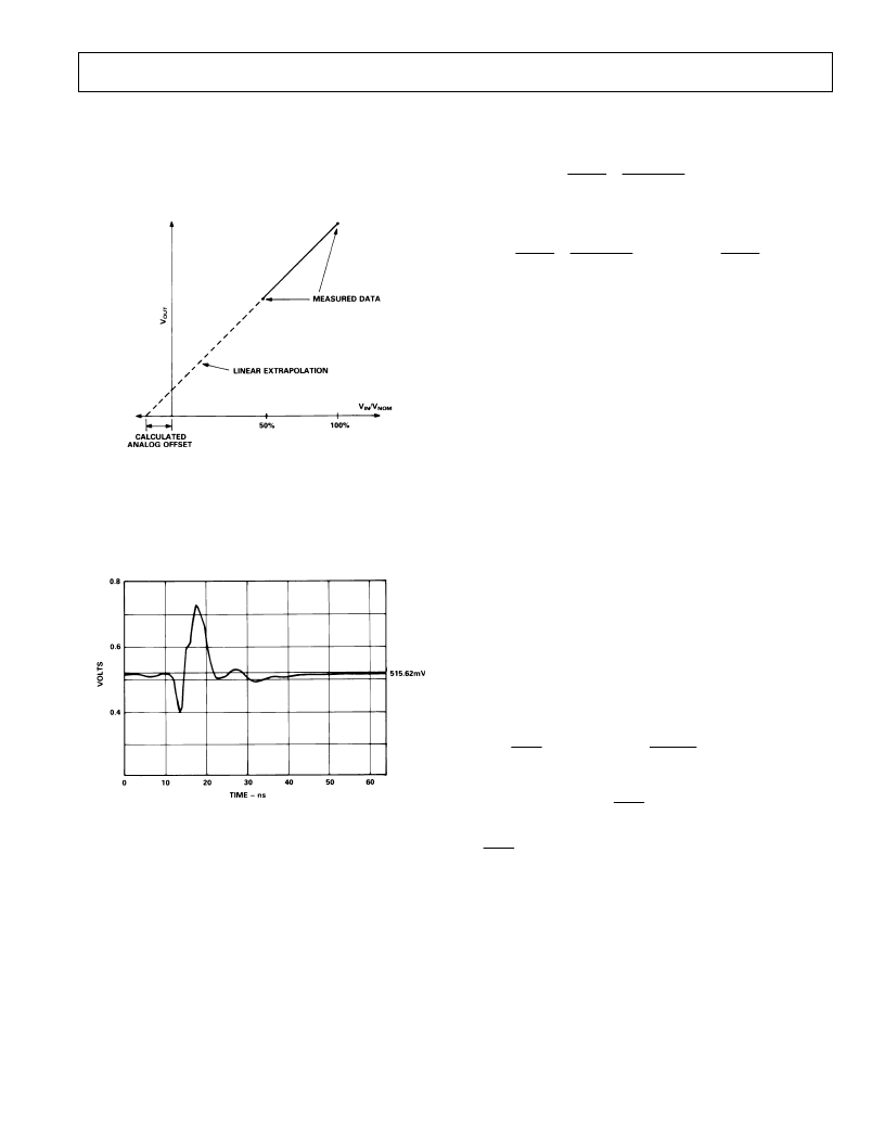
ANALOG OFFSET ERROR: The analog offset is defined as
the offset of the analog amplifier channel, referred to the analog
input. Ideally, this would be measured with the analog input at
0 V and the digital input at full scale. Since a 0 V analog input
voltage constitutes an undervoltage condition, this specification
is determined through linear extrapolation, as indicated in
Figure 1.
Figure 1. Derivation of Analog Offset Voltage
GLITCH IMPULSE: Asymmetrical switching times in a DAC
may give rise to undesired output transients which are quanti-
fied by their glitch impulse. It is specified as the net area of the
glitch in pV-sec.
Figure 2. AD668 Major Carry Glitch
FUNCTIONAL DESCRIPTION
The AD668 is designed to combine excellent performance with
maximum flexibility. The functional block diagram and the
simple transfer functions provided below will provide the user
with a basic grasp of the AD668’s operation. Examples of typi-
cal circuit configurations are provided in the section APPLY-
ING THE AD668. Subsequent sections contain more detailed
information useful in optimizing DAC performance in high
speed, high resolution applications.
DAC Transfer Function
The AD668 may be used either in a current output mode (DAC
output connected to a virtual ground) or a voltage output mode
(DAC output connected to a resistive load).
In current output mode:
Unipolar Mode
I
OUT
=
V
IN
V
NOM
×
DAC code
4096
×
10.24
mA
Bipolar Mode
I
OUT
=
V
IN
V
NOM
×
DAC code
4096
×
10.24
mA
–
V
IN
V
NOM
×
5.12
mA
In voltage output mode:
V
OUT
=
I
OUT
×
R
LOAD
(for both unipolar and bipolar modes)
where:
V
IN
– the analog input voltage.
V
NOM
–
the nominal full scale of the reference voltage: 1 V,
1.25 V, or 5 V, determined by the wiring configuration of Pins
21 and 22. (See APPLYING THE AD668.)
DAC code –
the numerical representation of the DAC’s digital
inputs; a number between 0 and 4095.
R
LOAD
–
the resistance of the DAC output node; the maximum
this can be is 200
(the internal DAC ladder resistance). The
on-board load resistor (Pin 19) has been trimmed so that its
parallel combination with the DAC ladder resistance is 100
(
±
1%)
Bipolar mode –
produces a bipolar analog output from the digital
input by offsetting the normal output current with a precision
current source. This offset is achieved by connecting Pin 16 to
the DAC output. In the unipolar mode, Pin 16 should be
grounded.
If the dc errors are included, the transfer function becomes
somewhat more complex:
I
OUT
=
V
IN
V
NOM
+
OFFSET
ANALOG
×
DAC code
4096
×
(1
+
E
)
×
10.24
mA
+
OFFSET
DIGITAL
×
V
IN
V
NOM
×
10.24
mA
–
V
IN
V
NOM
+
OFFSET
ANALOG
×
(5.12
mA
+
[
OFFSET
BIPOLAR
×
10.24
mA
])
(Last term is for use in bipolar mode; V
OUT
is still just I
OUT
×
R
LOAD
)
where:
OFFSET
ANALOG
=
the analog offset error.
OFFSET
DIGITAL
= is
the unipolar digital offset error.
OFFSET
BIPOLAR
= is
the bipolar offset error.
E
= the gain error, expressed fractionally.
Operating Limits:
相關(guān)PDF資料 |
PDF描述 |
|---|---|
| AD668J | 12-Bit Ultrahigh Speed Multiplying D/A Converter |
| AD668K | 12-Bit Ultrahigh Speed Multiplying D/A Converter |
| AD668KQ | RES 36.0 OHM 1/8W 1% 0805 SMD |
| AD668S | 12-Bit Ultrahigh Speed Multiplying D/A Converter |
| AD668SQ | 12-Bit Ultrahigh Speed Multiplying D/A Converter |
相關(guān)代理商/技術(shù)參數(shù) |
參數(shù)描述 |
|---|---|
| AD668J | 制造商:AD 制造商全稱:Analog Devices 功能描述:12-Bit Ultrahigh Speed Multiplying D/A Converter |
| AD668JQ | 制造商:Analog Devices 功能描述:DAC 1-CH R-2R/Current Steering 12-bit 24-Pin CDIP Tube |
| AD668K | 制造商:AD 制造商全稱:Analog Devices 功能描述:12-Bit Ultrahigh Speed Multiplying D/A Converter |
| AD668KQ | 制造商:Analog Devices 功能描述: 制造商:Rochester Electronics LLC 功能描述: |
| AD668S | 制造商:AD 制造商全稱:Analog Devices 功能描述:12-Bit Ultrahigh Speed Multiplying D/A Converter |
發(fā)布緊急采購(gòu),3分鐘左右您將得到回復(fù)。