- 您現(xiàn)在的位置:買賣IC網(wǎng) > Datasheet目錄38 > AD650SD (Analog Devices Inc)IC V-F/F-V CONV 1MHZ 14-CDIP Datasheet資料下載
參數(shù)資料
| 型號(hào): | AD650SD |
| 廠商: | Analog Devices Inc |
| 文件頁數(shù): | 17/20頁 |
| 文件大?。?/td> | 385K |
| 描述: | IC V-F/F-V CONV 1MHZ 14-CDIP |
| 標(biāo)準(zhǔn)包裝: | 1 |
| 類型: | 電壓至頻率和頻率至電壓 |
| 頻率 - 最大: | 1MHz |
| 全量程: | ±150ppm/°C |
| 線性: | ±0.1% |
| 安裝類型: | 通孔 |
| 封裝/外殼: | 14-CDIP(0.300",7.62mm) |
| 供應(yīng)商設(shè)備封裝: | 14-CDIP |
| 包裝: | 管件 |
Data Sheet
AD650
Rev. E | Page 17 of 20
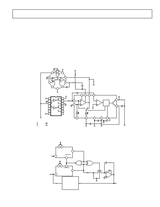
PHASE-LOCKED LOOP F/V CONVERSION
Although the F/V conversion technique shown in Figure 13 is
quite accurate and uses only a few extra components, it is very
limited in terms of signal frequency response and carrier feed-
through. If the carrier (or input) frequency changes
instantaneously, then the output cannot change very rapidly due
to the integrator time constant formed by CINT and RIN. While it
is possible to decrease the integrator time constant to provide
faster settling of the F-to-V output voltage, the carrier
feedthrough then becomes larger. For signal frequency response
in excess of 2 kHz, a phase-locked F/V conversion technique
such as the one shown in Figure 22 is recommended.
In a phase-locked loop circuit, the oscillator is driven to a
frequency and phase equal to an input reference signal. In
applications such as a synthesizer, the oscillator output
frequency is first processed through a programmable
divide by
N
before being applied to the phase detector as feedback. Here
the oscillator frequency is forced to be equal to
N times
the
reference frequency. It is this frequency output that is the
desired output signal and not a voltage. In this case, the AD650
offers compact size and wide dynamic range.
14
13
1
8
6
5
4
2
3
7
9
10
1
2
5
4
3
6
+V
S
V
S
+V
S
AD582
V
S
1000pF
CAP
0.1礔
200k&
10k&
OUTPUT
1k&
1
2
3
4
14
13
12
11
5
10
6
9
7
8
AD7512
V
S
+V
S
CONTROL
INPUT
+5V
INPUT
VOLTAGE
16.9k&
0.5mA
BIPOLAR
OFFSET
1mA
V
S
+IN
IN
+V
S
C
OS
NULL
AD650
COMPARATOR
INPUT
COMPARATOR
FREQUENCY
OUTPUT
DIGITAL
GND
ANALOG
GND
FREQUENCY
OUTPUT
ONE
SHOT
OP
AMP
0.6 VOLT
500&
10礔
0.1礔
51pF
0.1礔
+
10
15V +15V
GND
1000pF
9
3.6k&
5 VOLTS VFC NORMAL
GND AUTO ZERO
11
12
8
Figure 21. Autozero Circuit
C
51pF
15pF
R
140k&
71.5k&
590k&
15V
10
12
4
1
2
11
3
13
9
5
AD650
1MHz FULL-SCALE
R
IN
= 16.9k
C
OS
= 51pF
C
INT
= 1000pF
(UNIPOLAR INPUT)
FREQ
OUT
INPUT
CARRIER
VOLTS INPUT
TO AD650
NAND
XOR
1
2
5
4
3
6
G
D
B
S
1/2 7474
1/2 7474
D
1
PR
1
D
2
PR
2
Q
1
Q
2
CLEAR
1
SD211
DMOSFET
D TYPE FLIP FLOP
1
1
F/V
VOLTAGE
OUTPUT
INPUT
CARRIER
CLOCK
1
CLOCK
2
CLEAR
2
AD509
OPAMP
1/4 7400
7486
Figure 22. Phase-Locked Loop F/V Conversion
相關(guān)PDF資料 |
PDF描述 |
|---|---|
| AD652SQ | IC V-F CONV SYNCH MONO 5V 16CDIP |
| AD654JNZ/+ | IC CONV VOLT-FREQ 500KHZ 8DIP |
| AD7740YRM | IC CONVERTER V TO FREQ 8-MSOP |
| ADM1070ARTZ-REEL7 | IC CTRLR HOTSWAP -48V SOT23-6 |
| ADM1073ARU-REEL | IC CTRLR HOTSWAP -48V 14TSSOP |
相關(guān)代理商/技術(shù)參數(shù) |
參數(shù)描述 |
|---|---|
| AD650SD/883B | 功能描述:電壓頻率轉(zhuǎn)換及頻率電壓轉(zhuǎn)換 IC - V/F CONVERTER IC RoHS:否 制造商:Texas Instruments 全標(biāo)度頻率:4000 KHz 線性誤差:+/- 1 % FSR 電源電壓-最大: 電源電壓-最小: 最大工作溫度:+ 85 C 最小工作溫度:- 25 C 安裝風(fēng)格:Through Hole 封裝 / 箱體:PDIP-14 封裝:Tube |
| AD650SD-883B | 制造商:AD 制造商全稱:Analog Devices 功能描述:Voltage-to-Frequency and Frequency-to-Voltage Converter |
| AD650TYHHLBOX | 制造商:Advanced Micro Devices 功能描述:AMD A-SERIES APU A8-6500T X4 3100MHZ 4MB FM2 45W PIB - Boxed Product (Development Kits) |
| AD651AQ | 制造商:未知廠家 制造商全稱:未知廠家 功能描述:Converter |
| AD651SQ | 制造商:Rochester Electronics LLC 功能描述:- Bulk |
發(fā)布緊急采購,3分鐘左右您將得到回復(fù)。