- 您現(xiàn)在的位置:買賣IC網(wǎng) > PDF目錄373868 > AD4360-8 (Analog Devices, Inc.) Integrated Synthesizer and VCO PDF資料下載
參數(shù)資料
| 型號(hào): | AD4360-8 |
| 廠商: | Analog Devices, Inc. |
| 元件分類: | XO, clock |
| 英文描述: | Integrated Synthesizer and VCO |
| 中文描述: | 綜合合成器和VCO |
| 文件頁數(shù): | 11/24頁 |
| 文件大小: | 332K |
| 代理商: | AD4360-8 |
ADF4360-8
Lock Detect
MUXOUT can be programmed for one type of lock detect.
Digital lock detect is active high. When LDP in the R counter
latch is set to 0, digital lock detect is set high when the phase error
on three consecutive phase detector cycles is less than 15 ns.
Rev. A | Page 11 of 24
With LDP set to 1, five consecutive cycles of less than 15 ns
phase error are required to set the lock detect. It stays set high
until a phase error of greater than 25 ns is detected on any
subsequent PD cycle.
INPUT SHIFT REGISTER
The ADF4360 family’s digital section includes a 24-bit input
shift register, a 14-bit R counter, and an 18-bit N counter
comprised of a 5-bit A counter and a 13-bit B counter. Data is
clocked into the 24-bit shift register on each rising edge of CLK.
The data is clocked in MSB first. Data is transferred from the
shift register to one of four latches on the rising edge of LE. The
destination latch is determined by the state of the two control
bits (C2, C1) in the shift register. The two LSBs, DB1 and DB0,
are shown in Figure 2.
The truth table for these bits is shown in Table 5. Table 6 shows
a summary of how the latches are programmed. Note that the
test modes latch is used for factory testing and should not be
programmed by the user.
Table 5. C2 and C1 Truth Table
Control Bits
C2
C1
Data Latch
0
0
Control Latch
0
1
R Counter
1
0
N Counter (B)
1
1
Test Modes Latch
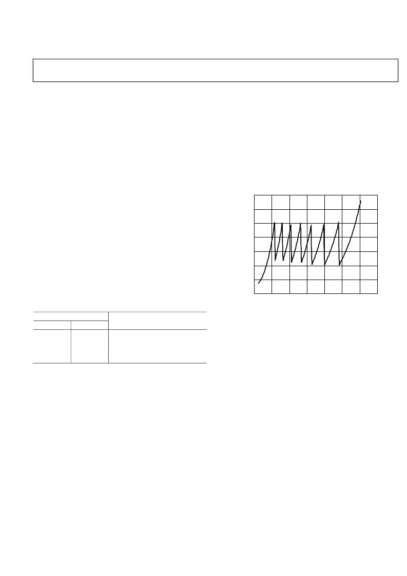
VCO
The VCO core in the ADF4360 family uses eight overlapping
bands, as shown in Figure 19, to allow a wide frequency range to
be covered without a large VCO sensitivity (K
V
) and resultant
poor phase noise and spurious performance.
The correct band is chosen automatically by the band select
logic at power-up or whenever the N counter latch is updated. It
is important that the correct write sequence be followed at
power-up. This sequence is
1.
2.
3.
R counter latch
Control latch
N counter latch
During band select, which takes five PFD cycles, the VCO V
TUNE
is disconnected from the output of the loop filter and connected
to an internal reference voltage.
0
1.0
0.5
2.5
2.0
1.5
3.5
3.0
80
85
90
100
95
105
115
110
FREQUENCY (MHz)
V
T
0
Figure 19. Frequency vs. V
TUNE
, ADF4360-8, L1 and L2 = 270 nH
The R counter output is used as the clock for the band select
logic and should not exceed 1 MHz. A programmable divider is
provided at the R counter input to allow division by 1, 2, 4, or 8,
and is controlled by the BSC1 bit and the BSC2 bit in the R
counter latch. Where the required PFD frequency exceeds
1 MHz, the divide ratio should be set to allow enough time for
correct band selection.
After band selection, normal PLL action resumes. The value of
K
V
is determined by the value of inductors used (see the
Choosing the Correct Inductance Value section). The ADF4360
family contains linearization circuitry to minimize any variation
of the product of I
CP
and K
V
.
The operating current in the VCO core is programmable in four
steps: 2.5 mA, 5 mA, 7.5 mA, and 10 mA. This is controlled by
the PC1 bit and the PC2 bit in the control latch.
相關(guān)PDF資料 |
PDF描述 |
|---|---|
| AD45048ARZ-REEL | Rail-to-Rail Upstream ADSL Line Driver |
| AD45048ARZ-REEL7 | Rail-to-Rail Upstream ADSL Line Driver |
| AD45048AR-REEL | Rail-to-Rail Upstream ADSL Line Driver |
| AD45048AR-REEL7 | Rail-to-Rail Upstream ADSL Line Driver |
| AD45048 | Rail-to-Rail Upstream ADSL Line Driver |
相關(guān)代理商/技術(shù)參數(shù) |
參數(shù)描述 |
|---|---|
| AD43ABS | 制造商:POP 功能描述: 制造商:RIVETS 功能描述: |
| AD43BS | 制造商:POP 功能描述: 制造商:RIVETS 功能描述: |
| AD43BSLF | 制造商:POP 功能描述: |
| AD43H | 制造商:POP 功能描述: |
| AD44 | 制造商:SMC Corporation of America 功能描述:BOWL, AUTO DRAIN FILTER FOR AF4000 制造商:MQP (ELECTRONICS) 功能描述:ADAPTOR DIL 40WAY |
發(fā)布緊急采購,3分鐘左右您將得到回復(fù)。