- 您現(xiàn)在的位置:買賣IC網(wǎng) > PDF目錄122717 > 935267488112 (NXP SEMICONDUCTORS) 8-BIT, OTPROM, 20 MHz, MICROCONTROLLER, PDSO20 PDF資料下載
參數(shù)資料
| 型號(hào): | 935267488112 |
| 廠商: | NXP SEMICONDUCTORS |
| 元件分類: | 微控制器/微處理器 |
| 英文描述: | 8-BIT, OTPROM, 20 MHz, MICROCONTROLLER, PDSO20 |
| 封裝: | 7.50 MM, PLASTIC, SO-20 |
| 文件頁(yè)數(shù): | 53/69頁(yè) |
| 文件大?。?/td> | 352K |
| 代理商: | 935267488112 |
第1頁(yè)第2頁(yè)第3頁(yè)第4頁(yè)第5頁(yè)第6頁(yè)第7頁(yè)第8頁(yè)第9頁(yè)第10頁(yè)第11頁(yè)第12頁(yè)第13頁(yè)第14頁(yè)第15頁(yè)第16頁(yè)第17頁(yè)第18頁(yè)第19頁(yè)第20頁(yè)第21頁(yè)第22頁(yè)第23頁(yè)第24頁(yè)第25頁(yè)第26頁(yè)第27頁(yè)第28頁(yè)第29頁(yè)第30頁(yè)第31頁(yè)第32頁(yè)第33頁(yè)第34頁(yè)第35頁(yè)第36頁(yè)第37頁(yè)第38頁(yè)第39頁(yè)第40頁(yè)第41頁(yè)第42頁(yè)第43頁(yè)第44頁(yè)第45頁(yè)第46頁(yè)第47頁(yè)第48頁(yè)第49頁(yè)第50頁(yè)第51頁(yè)第52頁(yè)當(dāng)前第53頁(yè)第54頁(yè)第55頁(yè)第56頁(yè)第57頁(yè)第58頁(yè)第59頁(yè)第60頁(yè)第61頁(yè)第62頁(yè)第63頁(yè)第64頁(yè)第65頁(yè)第66頁(yè)第67頁(yè)第68頁(yè)第69頁(yè)
Philips Semiconductors
Preliminary specification
87LPC768
Low power, low price, low pin count (20 pin) microcontroller with
4 kB OTP 8-bit A/D, Pulse Width Modulator
2000 May 02
55
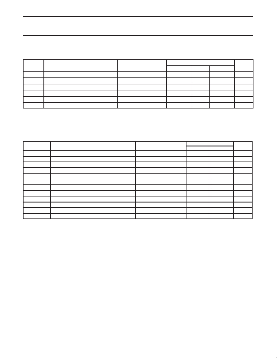
COMPARATOR ELECTRICAL CHARACTERISTICS
VDD = 3.0 V to 6.0 V unless otherwise specified; Tamb = 0°C to +70°C or –40°C to +85°C, unless otherwise specified
SYMBOL
PARAMETER
TEST CONDITIONS
LIMITS
UNIT
SYMBOL
PARAMETER
TEST CONDITIONS
MIN
TYP
MAX
UNIT
VIO
Offset voltage comparator inputs1
±10
mV
VCR
Common mode range comparator inputs
0
VDD–0.3
V
CMRR
Common mode rejection ratio1
–50
dB
Response time
250
500
ns
Comparator enable to output valid
10
s
IIL
Input leakage current, comparator
0 < VIN < VDD
±10
A
NOTE:
1. This parameter is guaranteed by characterization, but not tested in production.
A/D CONVERTER DC ELECTRICAL CHARACTERISTICS
Vdd = 3.0V to 6.0V unless otherwise specified;
Tamb = 0 to +70
°C for commercial, -40°C to +85°C for industrial, unless otherwise specified.
SYMBOL
PARAMETER
TEST CONDITIONS
LIMITS
UNIT
SYMBOL
PARAMETER
TEST CONDITIONS
MIN
MAX
UNIT
AVIN
Analog input voltage
VSS - 0.2
VDD + 0.2
V
RREF
Resistance between VDD and VSS
A/D enabled
tbd
k
CIA
Analog input capacitance
15
pF
DLe
Differential non-linearity1,2,3
±1
LSB
ILe
Integral non-linearity1,4
±1
LSB
OSe
Offset error1,5
±2
LSB
Ge
Gain error1,6
±1
%
Ae
Absolute voltage error1,7
±1
LSB
MCTC
Channel-to-channel matching
±1
LSB
Ct
Crosstalk between inputs of port8
0 - 100kHz
-60
dB
-
Input slew rate
100
V/ms
-
Input source impedance
10
k
NOTES:
1. Conditions: VSS = 0V; VDD = 5.12V.
2. The A/D is monotonic, there are no missing codes
3. The differential non-linearity (DLe) is the difference between the actual step width and the ideal step width. See Figure 41.
4. The integral non-linearity (ILe) is the peak difference between the center of the steps of the actual and the ideal transfer curve after
appropriate adjustment of gain and offset errors. See Figure 41.
5. The offset error (OSe) is the absolute difference between the straight line which fits the actual transfer curve (after removing gain error), and
the straight line which fits the ideal transfer curve. See Figure 41.
6. The gain error (Ge) is the relative difference in percent between the straight line fitting the actual transfer curve (after removing offset error),
and the straight line which fits the ideal transfer curve. Gain error is constant at every point on the transfer curve. See Figure 41.
7. The absolute voltage error (Ae) is the maximum difference between the center of the steps of the actual transfer curve of the non-calibrated
ADC and the ideal transfer curve.
8. This should be considered when both analog and digital signals are input simultaneously to A/D pins.
9. Changing the input voltage faster than this may cause erroneous readings.
10. A source impedance higher than this driving an A/D input may result in loss of precision and erroneous readings.
相關(guān)PDF資料 |
PDF描述 |
|---|---|
| 9ERS3165BGILF | 400 MHz, PROC SPECIFIC CLOCK GENERATOR, PDSO64 |
| 9LPRS535BFLFT | SPECIALTY MICROPROCESSOR CIRCUIT, PDSO48 |
| 935208500112 | 8-BIT, 16 MHz, MICROCONTROLLER, PDIP40 |
| 935208540112 | 8-BIT, 16 MHz, MICROCONTROLLER, PQCC44 |
| 935267591518 | 8-BIT, MROM, 16 MHz, MICROCONTROLLER, PQFP44 |
相關(guān)代理商/技術(shù)參數(shù) |
參數(shù)描述 |
|---|---|
| 935268081112 | 制造商:NXP Semiconductors 功能描述:SUB ONLY IC |
| 935268721125 | 制造商:NXP Semiconductors 功能描述:Buffer/Line Driver 1-CH Non-Inverting 3-ST CMOS 5-Pin TSSOP T/R |
| 935269304128 | 制造商:ST-Ericsson 功能描述:IC AUDIO CODEC W/TCH SCRN 48LQFP |
| 935269544557 | 制造商:NXP Semiconductors 功能描述:SUB ONLY TDA9587-2US1-V1.3 |
| 935269987557 | 制造商:NXP Semiconductors 功能描述:SUB ONLY TDA9587-1US1-V1.8 SUBBED TO 935269987557 |
發(fā)布緊急采購(gòu),3分鐘左右您將得到回復(fù)。