- 您現(xiàn)在的位置:買賣IC網(wǎng) > PDF目錄378217 > 82801E (INTEL CORP) Intel 82801E Communications I/O Controller Hub (C-ICH) PDF資料下載
參數(shù)資料
| 型號: | 82801E |
| 廠商: | INTEL CORP |
| 元件分類: | 外設(shè)及接口 |
| 英文描述: | Intel 82801E Communications I/O Controller Hub (C-ICH) |
| 中文描述: | MULTIFUNCTION PERIPHERAL, PBGA421 |
| 封裝: | BGA-421 |
| 文件頁數(shù): | 47/84頁 |
| 文件大小: | 1196K |
| 代理商: | 82801E |
第1頁第2頁第3頁第4頁第5頁第6頁第7頁第8頁第9頁第10頁第11頁第12頁第13頁第14頁第15頁第16頁第17頁第18頁第19頁第20頁第21頁第22頁第23頁第24頁第25頁第26頁第27頁第28頁第29頁第30頁第31頁第32頁第33頁第34頁第35頁第36頁第37頁第38頁第39頁第40頁第41頁第42頁第43頁第44頁第45頁第46頁當(dāng)前第47頁第48頁第49頁第50頁第51頁第52頁第53頁第54頁第55頁第56頁第57頁第58頁第59頁第60頁第61頁第62頁第63頁第64頁第65頁第66頁第67頁第68頁第69頁第70頁第71頁第72頁第73頁第74頁第75頁第76頁第77頁第78頁第79頁第80頁第81頁第82頁第83頁第84頁
Intel
82801E C-ICH
Advance Information Datasheet
47
3.2.18
Miscellaneous Signals
3.2.19
General Purpose I/O
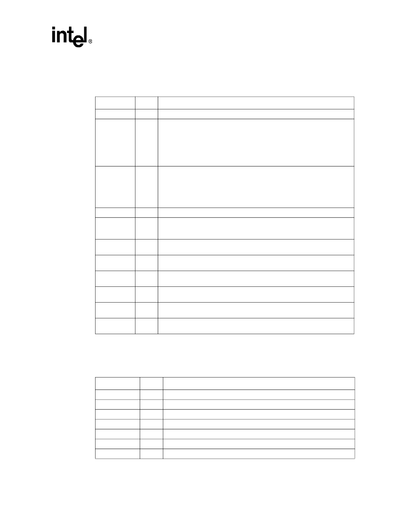
Table 24. Miscellaneous Signals
Name
Type
Description
HL[11]
I
No pull-up required. Use a no-stuff or a test point for NAND tree testing.
RTCRST#
I
RTC Reset:
When asserted, this signal resets register bits in the RTC well and
sets the RTC_PWR_STS bit (bit 2 in GEN_PMCON3 register). This signal is also
used to enter the test modes documented in
“Test Signals” on page 49.
NOTE:
Clearing CMOS in an 82801E C-ICH-based platform can be done by
using a jumper on RTCRST# or GPI, or using SAFEMODE strap.
Implementations should not attempt to clear CMOS by using a jumper to
pull VccRTC low.
SPKR
O
Speaker:
The SPKR signal is the output of counter 2 and is internally ANDed with
Port 61h bit 1 to provide Speaker Data Enable. This signal drives an external
speaker driver device, which in turn drives the system speaker. Upon PCIRST#, its
output state is 1.
NOTE:
SPKR is sampled at the rising edge of PWROK as a functional strap. See
“Functional Straps” on page 49for more details.
TP0
I
Test Point 0:
This signal must have an external pull-up to Vcc3_3.
THRM#
I
Thermal Alarm:
THRM# is an active low signal generated by external hardware to
start the hardware clock throttling mode. This signal can also generate an SMI# or
an SCI.
RI#
I
Ring Indicate:
From the modem interface. This signal can be enabled as a wake
event; this is preserved across power failures.
RESERVED1
RESERVED2
—
This signal must have an external pull up to Vcc3_3.
SUSCLK
O
Suspend Clock:
This signal is an output of the RTC generator circuit and is used
by other chips for the refresh clock.
TP1
I
Test Point 1:
Route to a test point with option to jumper to Vcc1_8. Used for
NAND tree testing. Otherwise jumper to Vcc1_8.
TP2
I
Test Point 2:
Route to a test point with option to jumper to V
SS
. Used for NAND
tree testing. Otherwise jumper to V
SS
.
TP3
I
Test Point 3:
Route to a test point with option to jumper to V
SS
. Used for NAND
tree testing. Otherwise jumper to V
SS
.
Table 25. General Purpose I/O Signals (Sheet 1 of 2)
Name
Type
Description
GPIO[31:29]
O
Not implemented.
GPIO[28:27]
I/O
Can be input or output. Main power well. Unmuxed.
GPIO[26]
I/O
Not implemented.
GPIO[25]
I/O
Can be input or output. Main power well. Not Muxed.
GPIO[24]
I/O
Can be input or output. Main power well.
GPIO[23]
O
Fixed as Output only. Main power well.
GPIO[22]
OD
Fixed as Output only. Main power well. Open-drain output.
相關(guān)PDF資料 |
PDF描述 |
|---|---|
| 82802AB | Firmware Hub (FWH) |
| 82802AC | Firmware Hub (FWH) |
| 8281 | LNB SUPPLY AND CONTROL-VOLTAGE REGULATORS |
| 8282 | OCTAL LATCH |
| 8282 | LNB SUPPLY AND CONTROL-VOLTAGE REGULATORS |
相關(guān)代理商/技術(shù)參數(shù) |
參數(shù)描述 |
|---|---|
| 82801FB | 制造商:INTEL 制造商全稱:Intel Corporation 功能描述:Intel I/O Controller Hub 6 (ICH6) Family |
| 82801FBM | 制造商:INTEL 制造商全稱:Intel Corporation 功能描述:Intel I/O Controller Hub 6 (ICH6) Family |
| 82801FR | 制造商:INTEL 制造商全稱:Intel Corporation 功能描述:Intel I/O Controller Hub 6 (ICH6) Family |
| 82801GBICH7 | 制造商:INTEL 制造商全稱:Intel Corporation 功能描述:Intel I/O Controller Hub 7 |
| 82801GBMICH7-M | 制造商:INTEL 制造商全稱:Intel Corporation 功能描述:Intel I/O Controller Hub 7 |
發(fā)布緊急采購,3分鐘左右您將得到回復(fù)。