- 您現(xiàn)在的位置:買賣IC網(wǎng) > PDF目錄360443 > 74F760 (NXP Semiconductors N.V.) Octal buffer (open-collector)(八通道緩沖器(集電極開路)) PDF資料下載
參數(shù)資料
| 型號: | 74F760 |
| 廠商: | NXP Semiconductors N.V. |
| 英文描述: | Octal buffer (open-collector)(八通道緩沖器(集電極開路)) |
| 中文描述: | 八路緩沖器(集電極開路)(八通道緩沖器(集電極開路)) |
| 文件頁數(shù): | 9/14頁 |
| 文件大?。?/td> | 128K |
| 代理商: | 74F760 |
Philips Semiconductors
Application note
AN214
74F extended octal-plus family applications
June 1988
9
74F657 Operation
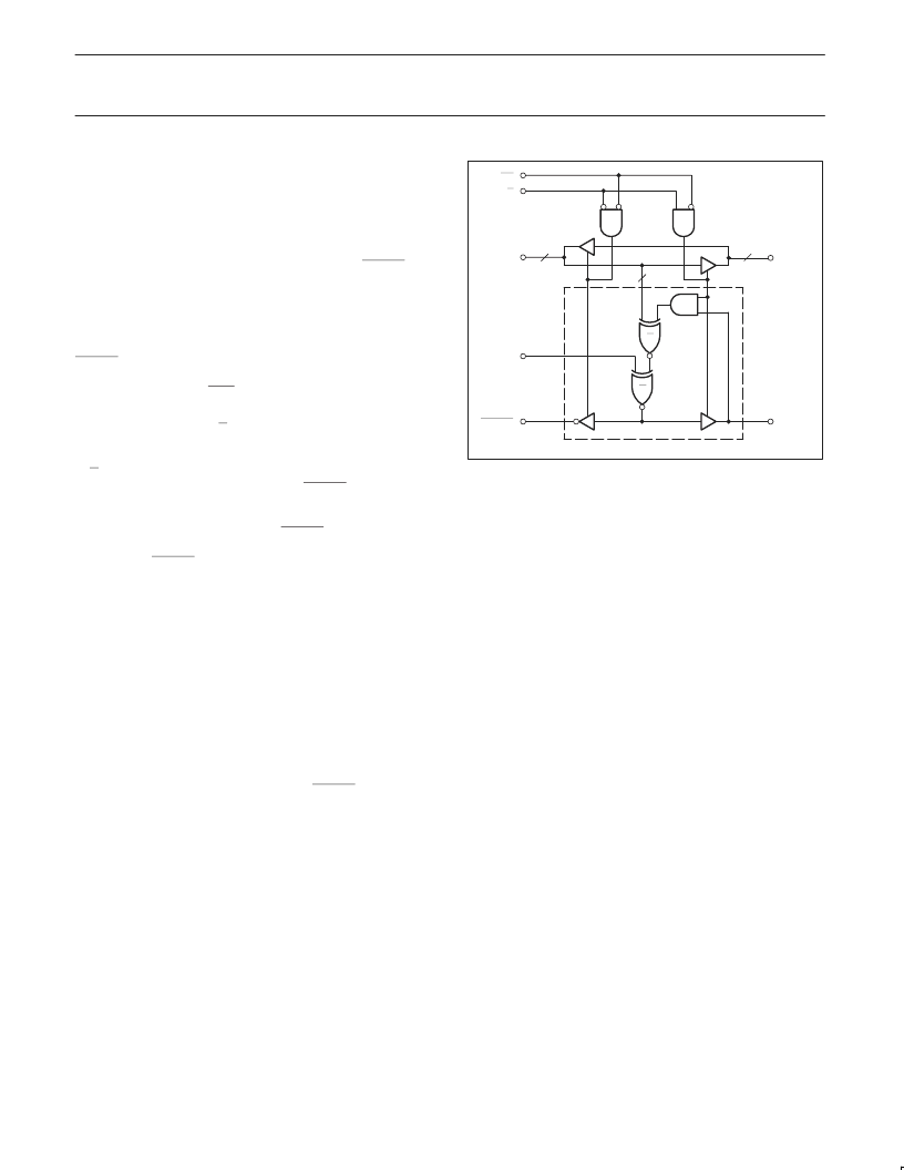
The 74F657 Parity Bus Transceiver, as shown in its simplified logic
diagram, Figure 10, is a combination of a 74F245 Octal Transceiver
and a 74F280B 9-bit Parity Generator/Checker plus one AND gate.
Figure 11 expands the logic block diagram of the Family’s Parity
Tree Logic (inside the dashed line of Figure 10).
During TRANSMIT mode (A
N
= Hi-Z), the PARITY and ERROR
outputs are generated from the A
N
input/output port. In the
RECEIVE mode, the B
N
port is the input from the system or mother
board bus (B-port outputs = Hi-Z).
For best speed performance, PARITY should always be generated
from the A
N
port for the B
N
port (TRANSMIT mode), and parity
ERROR should always be checked for data coming in on the B-port
(RECEIVE mode). EVEN or ODD parity generation and checking is
determined by the EVEN/ODD input (EVEN = HIGH, and
ODD = LOW).
In the TRANSMIT mode (T/R = HIGH), transmitted data travels from
the A-port to the B-port in less than 8.0ns generating a PARITY bit
output in less than 16.0ns. Whereas, in the RECEIVE mode
(T/R = LOW), received data traverses from the B-port to the A-port
path in, again, less than 8.0ns, but then the ERROR checking
output, being generated from the output data presented to the A-port
and the PARITY input, takes an additional 16.5ns or less to stabilize.
Therefore, the total RECEIVEd-data-to-ERROR checking output
propagation time is the sum of the B
N
-to-A
N
delay (8ns) and the
A
N
/PARITY-to-ERROR output delay (16.5ns) or 22.5ns.
However, in many cases, the propagation delay that has to be taken
into consideration does not have to include parity calculation time
and could be equal to that of just the transceiver part (8ns). This is
due to the fact that it may not be too late to interrupt whatever needs
to be interrupted in case of a parity error after the data has already
gone by (i.e., via late bus error).
Parity Tree Analysis
The basic 3-input Comparator Cell, inside the dashed line in
Figure 11, is used throughout the Parity Bus Series. If there are an
even number of HIGH inputs (0 or 2) the output of the 3-Input
Comparator Cell will be HIGH, while an odd number (1 or 3) will
produce an output LOW. The 74F657’s Parity Tree Logic, combines
four of the 3-Input Comparators with a 2-input comparator, a 2-input
AND gate and output buffers for PARITY and ERROR to produce
the complete parity generator/checker logic.
EO
A
N
A0–A7)
ERROR
⊕
⊕
RE
TE
PARITY
8L
B
(B0–B7)
T/R
8L
8X
8L
SF01337
Figure 10. 74F657 Simplified Block Diagram
The 74F588 IEEE-488 Octal Transceiver
The 74F588 is a non-inverting IEEE-488 standard transceiver
contains eight bidirectional 3-State buffers. The B
N
port outputs can
source/sink –15mA/64mA (guaranteed) and have series termination
resistors as specified in the IEEE-488 specification. The A
N
port,
which interfaces to the PC board or system logic bus, is guaranteed
to source/sink –3mA/24mA. The 74F588 pinout is identical to that of
the 74F545 Octal Transceiver with the IEEE-488 termination
resistors in series with the B
N
port.
相關(guān)PDF資料 |
PDF描述 |
|---|---|
| 74F30244 | Octal 30Ω line driver with enable,non-inverting (open collector)(帶使能30Ω的八線驅(qū)動器,同向(開啟集電極)) |
| 74F764-1 | DRAM dual-ported controllers |
| 74F764-1A | DRAM dual-ported controllers |
| 74F764-1N | DRAM dual-ported controllers |
| 74F765-1 | DRAM dual-ported controllers |
相關(guān)代理商/技術(shù)參數(shù) |
參數(shù)描述 |
|---|---|
| 74F760D | 制造商:SIG 功能描述: |
| 74F764-1 | 制造商:PHILIPS 制造商全稱:NXP Semiconductors 功能描述:DRAM dual-ported controllers |
| 74F764-1A | 制造商:PHILIPS 制造商全稱:NXP Semiconductors 功能描述:DRAM dual-ported controllers |
| 74F764-1N | 制造商:PHILIPS 制造商全稱:NXP Semiconductors 功能描述:DRAM dual-ported controllers |
| 74F765-1 | 制造商:PHILIPS 制造商全稱:NXP Semiconductors 功能描述:DRAM dual-ported controllers |
發(fā)布緊急采購,3分鐘左右您將得到回復(fù)。