- 您現(xiàn)在的位置:買賣IC網(wǎng) > PDF目錄298491 > 7130LA35TF8 (INTEGRATED DEVICE TECHNOLOGY INC) 1K X 8 DUAL-PORT SRAM, 35 ns, PQFP64 PDF資料下載
參數(shù)資料
| 型號: | 7130LA35TF8 |
| 廠商: | INTEGRATED DEVICE TECHNOLOGY INC |
| 元件分類: | SRAM |
| 英文描述: | 1K X 8 DUAL-PORT SRAM, 35 ns, PQFP64 |
| 封裝: | STQFP-64 |
| 文件頁數(shù): | 4/19頁 |
| 文件大?。?/td> | 153K |
| 代理商: | 7130LA35TF8 |
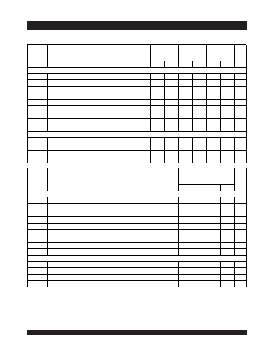
IDT7130SA/LA and IDT7140SA/LA
High-Speed 1K x 8 Dual-Port Static SRAM
Military, Industrial and Commercial Temperature Ranges
12
AC Electrical Characteristics Over the
Operating Temperature and Supply Voltage Range(7)
NOTES:
1.
PLCC, TQFP and STQFP packages only.
2.
Port-to-port delay through RAM cells from the writing port to the reading port, refer to “Timing Waveform of Write with Port -to-Port Read and
BUSY."
3.
To ensure that the earlier of the two ports wins.
4.
tBDD is a calculated parameter and is the greater of 0, tWDD – tWP (actual) or tDDD – tDW (actual).
5.
To ensure that a write cycle is inhibited on port 'B' during contention on port 'A'.
6.
To ensure that a write cycle is completed on port 'B' after contention on port 'A'.
7.
'X' in part numbers indicates power rating (S or L).
7130X20
(1)
7140X20
(1)
Com'l Only
7130X25
7140X25
Com'l, Ind
& Military
7130X35
7140X35
Com'l
& Military
Symbol
Parameter
Min.Max.Min.Max.Min.
Max.
Unit
BUSY TIMING (For MASTER IDT 7130)
tBAA
BUSY Access Time from Address
____
20
____
20
____
20
ns
tBDA
BUSY Disable Time from Address
____
20
____
20
____
20
ns
tBAC
BUSY Access Time from Chip Enable
____
20
____
20
____
20
ns
tBDC
BUSY Disable Time from Chip Enable
____
20
____
20
____
20
ns
tWH
Write Hold After
BUSY(6)
12
____
15
____
20
____
ns
tWDD
Write Pulse to Data Delay(2)
____
40
____
50
____
60
ns
tDDD
Write Data Valid to Read Data Delay(2)
____
30
____
35
____
35
ns
tAPS
Arbitration Priority Set-up Time
(3)
5
____
5
____
5
____
ns
tBDD
BUSY Disable to Valid Data(4)
____
25
____
35
____
35
ns
BUSY INPUT TIMING (For SLAVE IDT 7140)
tWB
Write to
BUSY Input(5)
0
____
0
____
0
____
ns
tWH
Write Hold After
BUSY(6)
12
____
15
____
20
____
ns
tWDD
Write Pulse to Data Delay
(2)
____
40
____
50
____
60
ns
tDDD
Write Data Valid to Read Data Delay(2)
____
30
____
35
____
35
ns
2689 tbl 11a
7130X55
7140X55
Com'l, Ind
& Military
7130X100
7140X100
Com'l, Ind
& Military
Symbol
Parameter
Min.
Max.
Min.
Max.
Unit
BUSY TIMING (For MASTER IDT 7130)
tBAA
BUSY Access Time from Address]
____
30
____
50
ns
tBDA
BUSY Disable Time from Address
____
30
____
50
ns
tBAC
BUSY Access Time from Chip Enable
____
30
____
50
ns
tBDC
BUSY Disable Time from Chip Enable
____
30
____
50
ns
tWH
Write Hold After
BUSY(6)
20
____
20
____
ns
tWDD
Write Pulse to Data Delay(2)
____
80
____
120
ns
tDDD
Write Data Valid to Read Data Delay
(2)
____
55
____
100
ns
tAPS
Arbitration Priority Set-up Time
(3)
5
____
5
____
ns
tBDD
BUSY Disable to Valid Data(4)
____
55
____
65
ns
BUSY INPUT TIMING (For SLAVE IDT 7140)
tWB
Write to
BUSY Input(5)
0
____
0
____
ns
tWH
Write Hold After
BUSY(6)
20
____
20
____
ns
tWDD
Write Pulse to Data Delay(2)
____
80
____
120
ns
tDDD
Write Data Valid to Read Data Delay
(2)
____
55
____
100
ns
2689 tbl 11b
相關(guān)PDF資料 |
PDF描述 |
|---|---|
| 7140LA35CB | 1K X 8 DUAL-PORT SRAM, 35 ns, CDIP48 |
| 7134SA35PB | 4K X 8 DUAL-PORT SRAM, 35 ns, PDIP48 |
| 71522-1050 | 50 CONTACT(S), MALE, TELECOM AND DATACOM CONNECTOR, IDC, PLUG |
| 71522-2050 | 50 CONTACT(S), MALE, TELECOM AND DATACOM CONNECTOR, IDC, PLUG |
| 71522-3050 | 50 CONTACT(S), MALE, TELECOM AND DATACOM CONNECTOR, IDC, PLUG |
相關(guān)代理商/技術(shù)參數(shù) |
參數(shù)描述 |
|---|---|
| 7130LA35TFG | 制造商:Integrated Device Technology Inc 功能描述:IC SRAM 8KBIT 35NS 64TQFP |
| 7130LA45TFI | 功能描述:IC SRAM 8KBIT 64TQFP 制造商:idt, integrated device technology inc 系列:* 零件狀態(tài):最後搶購 標(biāo)準(zhǔn)包裝:160 |
| 7130LA45TFI8 | 功能描述:IC SRAM 8KBIT 64TQFP 制造商:idt, integrated device technology inc 系列:* 零件狀態(tài):最後搶購 標(biāo)準(zhǔn)包裝:500 |
| 7130LA55C | 功能描述:靜態(tài)隨機(jī)存取存儲器 RoHS:否 制造商:Cypress Semiconductor 存儲容量:16 Mbit 組織:1 M x 16 訪問時(shí)間:55 ns 電源電壓-最大:3.6 V 電源電壓-最小:2.2 V 最大工作電流:22 uA 最大工作溫度:+ 85 C 最小工作溫度:- 40 C 安裝風(fēng)格:SMD/SMT 封裝 / 箱體:TSOP-48 封裝:Tray |
| 7130LA55CB | 功能描述:靜態(tài)隨機(jī)存取存儲器 RoHS:否 制造商:Cypress Semiconductor 存儲容量:16 Mbit 組織:1 M x 16 訪問時(shí)間:55 ns 電源電壓-最大:3.6 V 電源電壓-最小:2.2 V 最大工作電流:22 uA 最大工作溫度:+ 85 C 最小工作溫度:- 40 C 安裝風(fēng)格:SMD/SMT 封裝 / 箱體:TSOP-48 封裝:Tray |
發(fā)布緊急采購,3分鐘左右您將得到回復(fù)。