- 您現(xiàn)在的位置:買賣IC網(wǎng) > PDF目錄24691 > 05F8025 IC-SM-QUAD 12 BIT DAC PDF資料下載
參數(shù)資料
| 型號: | 05F8025 |
| 英文描述: | IC-SM-QUAD 12 BIT DAC |
| 中文描述: | 集成電路釤四路12位DAC |
| 文件頁數(shù): | 10/12頁 |
| 文件大小: | 502K |
| 代理商: | 05F8025 |

DAC8412/DAC8413
REV. C
–7–
ADDRESS
DECODE
INPUT
REG A
OUTPUT
REG A
*WRA
*RDA
12
DAC A
*RDD
*WRD
TO
AMPLIFIER
RESET
A0
A1
CS
R/W
DATA
LDAC
R/W
DECODE
*NOTE: THE SIGNALS RDA, WRA, ETC., ARE INTERNAL CONTROL SIGNALS.
THEY ARE INCLUDED FOR CLARIFICATION ONLY.
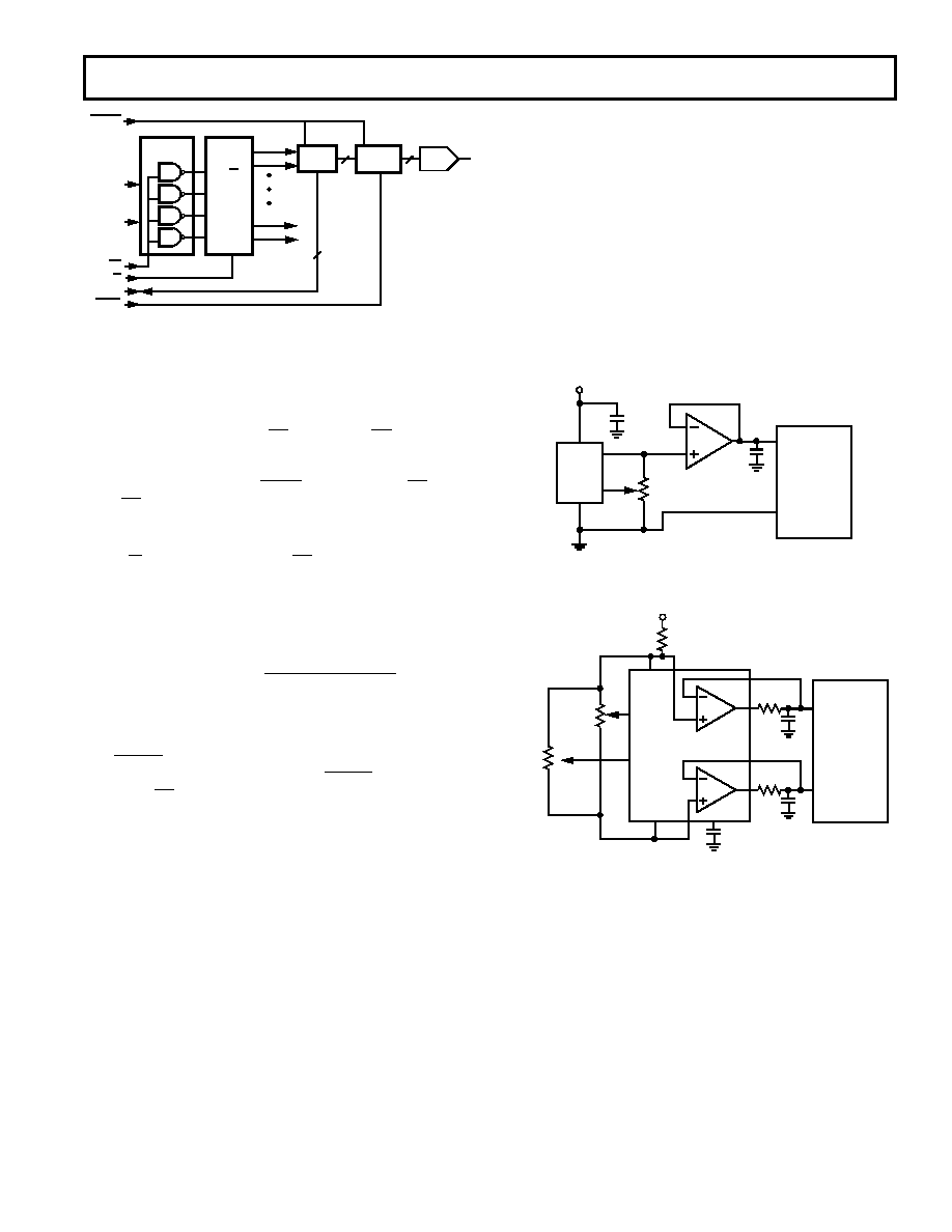
Figure 1. I/O Logic Diagram
See Figure 1 for a simplified I/O logic diagram. The register
select inputs A0 and A1 select individual DAC registers “A”
(binary code 00) through “D” (binary code 11). Decoding of
the registers is enabled by the CS input. When CS is high no
decoding takes place, and neither the writing nor the reading of
the input registers is enabled. The loading of the second bank of
registers is controlled by the LDAC input. By taking CS low
while CS is high, all output registers can be updated simulta-
neously. Note that the tLWD required pulse width for updating
all DACs is a minimum of 170 ns.
The R/W input, when enabled by CS, controls the writing to
and reading from the input register.
Coding
Both the DAC-8412 and DAC8413 use binary coding. The
output voltage can be calculated by:
V
OUT = VREFL +
(V
REFL _VREFL )* N
4096
where N is the digital code in decimal.
RESET
The RESET function can be used either at power-up or at any
time during the DAC’s operation. The RESET function is inde-
pendent of CS. This pin is active LOW and sets the DAC out-
put registers to either center code for the DAC8412, or zero
code for the DAC8413. The reset to center code is most useful
when the DAC is configured for bipolar references and an out-
put of zero volts after reset is desired.
Supplies
Supplies required are VSS, VDD and VLOGIC. The VSS supply can
be set between –15 volts and 0 volts. VDD is the positive supply;
its operating range is between +5 and +15 volts.
VLOGIC is the digital output reference voltage for the readback
function. It is normally connected to +5 volts. This pin is a
logic reference input only. It does not supply current to the de-
vice. If you are not using the readback function, VLOGIC can be
hardwired to VDD. While VLOGIC does not supply current to the
DAC8412, it does supply currents to the digital outputs when
readback is used.
Amplifiers
Unlike many voltage output DACs, the DAC8412 features buff-
ered voltage outputs. Each output is capable of both sourcing
and sinking 5 mA at
±10 volts, eliminating the need for external
amplifiers in most applications. These amplifiers are short cir-
cuit protected.
Careful attention to grounding is important to accurate opera-
tion of the DAC8412. This is not because the DAC8412 is
more sensitive than other 12-bit DACs, but because with four
outputs and two references there is greater potential for ground
loops. Since the DAC8412 has no analog ground, the ground
must be specified with respect to the reference.
Reference Configurations
Output voltage ranges can be configured as either unipolar or
bipolar, and within these choices a wide variety of options ex-
ists. The unipolar configuration can be either positive or nega-
tive voltage output, and the bipolar configuration can be either
symmetrical or nonsymmetrical.
OP-400
REF10
DAC8412
OR
DAC8413
+
+15V
INPUT
OUTPUT
TRIM
10k
V REFH
0.2
F
V REFL
+10V OPERATION
Figure 2. Unipolar +10 V Operation
DAC8412
OR
DAC8413
+15V
V REFH
1
F
±5 OR ±10V OPERATION
0.2
F
0.2
F
4
6
12
5
813
7
15
14
1
3
AD688 For
± 10v
AD588 For
± 5v
39k
6.2
6.2
V REFL
BALANCE
100k
GAIN
100k
Figure 3. Symmetrical Bipolar Operation
Figure 3 (Symmetrical Bipolar Operation) shows the DAC8412
configured for
±10 volt operation. Note: See the AD688 data
sheet for a full explanation of reference operation. Adjustments may
not be required for many applications since the AD688 is a very
high accuracy reference. However if additional adjustments are
required, adjust the DAC8412 full scale first. Begin by loading
the digital full-scale code (FFFH), and then adjust the Gain Ad-
just potentiometer to attain a DAC output voltage of 9.9976
volts. Then, adjust the Balance Adjust to set the center scale
output voltage to 0.000 volts.
The 0.2
F bypass capacitors shown at the reference inputs in
Figure 3 should be used whenever
±10 volt references are used.
Applications with single references or references to
±5 volts
may not require the 0.2
F bypassing. The 6.2 resistor in
series with the output of the reference amplifier is to keep the
amplifier from oscillating with the capacitive load. We have
相關(guān)PDF資料 |
PDF描述 |
|---|---|
| 05F8031 | IC-SM-QUAD 12 BIT DAC |
| 934051200112 | 40 MHz - 750 MHz RF/MICROWAVE WIDE BAND HIGH POWER AMPLIFIER |
| 934051230112 | 40 MHz - 750 MHz RF/MICROWAVE WIDE BAND HIGH POWER AMPLIFIER |
| 934051510185 | 100 mA, 50 V, PNP, Si, SMALL SIGNAL TRANSISTOR |
| 934031080215 | 100 mA, 50 V, PNP, Si, SMALL SIGNAL TRANSISTOR, TO-236AB |
相關(guān)代理商/技術(shù)參數(shù) |
參數(shù)描述 |
|---|---|
| 05FD101J03 | 制造商: 功能描述: 制造商:undefined 功能描述: |
| 05FD111J03 | 制造商: 功能描述: 制造商:undefined 功能描述: |
| 05FD161J03 | 制造商: 功能描述: 制造商:undefined 功能描述: |
| 05FD241J03 | 制造商: 功能描述: 制造商:undefined 功能描述: |
| 05FD271J03 | 制造商: 功能描述: 制造商:undefined 功能描述: |
發(fā)布緊急采購,3分鐘左右您將得到回復(fù)。